IEC 62899-203:2018
(Main)Printed electronics - Part 203: Materials - Semiconductor ink
Printed electronics - Part 203: Materials - Semiconductor ink
IEC 62899-203:2018(E) defines terms and specifies standard methods for characterisation and evaluation. This document is applicable to semiconductor inks and semiconductive layers that are made from semiconductor inks.
General Information
- Status
- Published
- Publication Date
- 27-Sep-2018
- Technical Committee
- TC 119 - Printed Electronics
- Drafting Committee
- WG 2 - TC 119/WG 2
- Current Stage
- DELPUB - Deleted Publication
- Start Date
- 28-May-2024
- Completion Date
- 30-Nov-2020
Relations
- Effective Date
- 05-Sep-2023
Overview
IEC 62899-203:2018 - Printed electronics - Part 203: Materials - Semiconductor ink - defines terms and specifies standard methods for the characterisation and evaluation of semiconductor inks and the semiconductive layers produced from them. Part of the IEC 62899 printed‑electronics series, this document provides standardized test conditions, measurement methods and storage/ageing guidance to ensure repeatable assessment of ink materials used in printed electronics.
Keywords: IEC 62899-203, semiconductor ink, printed electronics, characterisation, semiconductive layers, evaluation methods
Key Topics and Technical Requirements
The standard focuses on measurable properties and standard test procedures (see clause references in the document):
- Terms and definitions: clear definitions for “semiconductive material” and “semiconductor ink” aligned with IEC 62860.
- Atmospheric conditions: recommended conditioning and test atmosphere for reproducible results.
- Evaluation of ink composition:
- Solid content and non‑volatile content
- Density and evaporation characteristics
- Flash point and safety‑related properties
- Physical properties important for printing:
- Rheology (viscosity and flow behaviour)
- Surface tension
- Properties of formed semiconductive layers:
- Semiconductor type classification and test piece preparation (substrate, layer dimensions, processing)
- Electrical properties: charge mobility, dielectric behaviour, ionisation potential
- Optical properties: luminous transmittance, chromaticity, colour uniformity, haze, refractive index
- Storage and ageing: recommended storage conditions and methods to measure deterioration over time (including informative examples in Annex A and chromaticity test points in Annex B).
- Normative references: links to IEC 62860 and a range of ISO methods used for density, viscosity, refractive index, haze and colour measurements.
Practical Applications and Who Uses This Standard
IEC 62899-203 is intended for anyone involved in the development, supply, testing or procurement of semiconductor inks and printed semiconductive layers:
- Ink formulators and material suppliers - to characterize and certify ink batches
- Device manufacturers (printed transistors, sensors, OLEDs, flexible and wearable electronics) - for incoming inspection and process control
- Test laboratories and QA teams - to perform standardised measurements (rheology, mobility, optical metrics)
- R&D teams - to compare materials and report reproducible data
- Procurement and compliance - to specify material acceptance criteria
Related Standards
- IEC 62860 (characterization of organic transistors and materials)
- Relevant ISO standards referenced for density, viscosity, refractive index, haze, colourimetric and flash‑point measurements
Using IEC 62899-203 helps harmonize material data, improve reproducibility in printed electronics manufacturing, and support reliable selection of semiconductor inks for flexible, low-cost electronic applications.
Get Certified
Connect with accredited certification bodies for this standard

Intertek Testing Services NA Inc.
Intertek certification services in North America.

UL Solutions
Global safety science company with testing, inspection and certification.

ANCE
Mexican certification and testing association.
Sponsored listings
Frequently Asked Questions
IEC 62899-203:2018 is a standard published by the International Electrotechnical Commission (IEC). Its full title is "Printed electronics - Part 203: Materials - Semiconductor ink". This standard covers: IEC 62899-203:2018(E) defines terms and specifies standard methods for characterisation and evaluation. This document is applicable to semiconductor inks and semiconductive layers that are made from semiconductor inks.
IEC 62899-203:2018(E) defines terms and specifies standard methods for characterisation and evaluation. This document is applicable to semiconductor inks and semiconductive layers that are made from semiconductor inks.
IEC 62899-203:2018 is classified under the following ICS (International Classification for Standards) categories: 29.045 - Semiconducting materials; 87.080 - Inks. Printing inks. The ICS classification helps identify the subject area and facilitates finding related standards.
IEC 62899-203:2018 has the following relationships with other standards: It is inter standard links to IEC 62899-203:2024. Understanding these relationships helps ensure you are using the most current and applicable version of the standard.
IEC 62899-203:2018 is available in PDF format for immediate download after purchase. The document can be added to your cart and obtained through the secure checkout process. Digital delivery ensures instant access to the complete standard document.
Standards Content (Sample)
IEC 62899-203 ®
Edition 1.0 2018-09
INTERNATIONAL
STANDARD
colour
inside
Printed electronics –
Part 203: Materials – Semiconductor ink
All rights reserved. Unless otherwise specified, no part of this publication may be reproduced or utilized in any form
or by any means, electronic or mechanical, including photocopying and microfilm, without permission in writing from
either IEC or IEC's member National Committee in the country of the requester. If you have any questions about IEC
copyright or have an enquiry about obtaining additional rights to this publication, please contact the address below or
your local IEC member National Committee for further information.
IEC Central Office Tel.: +41 22 919 02 11
3, rue de Varembé info@iec.ch
CH-1211 Geneva 20 www.iec.ch
Switzerland
About the IEC
The International Electrotechnical Commission (IEC) is the leading global organization that prepares and publishes
International Standards for all electrical, electronic and related technologies.
About IEC publications
The technical content of IEC publications is kept under constant review by the IEC. Please make sure that you have the
latest edition, a corrigenda or an amendment might have been published.
IEC Catalogue - webstore.iec.ch/catalogue Electropedia - www.electropedia.org
The stand-alone application for consulting the entire The world's leading online dictionary of electronic and
bibliographical information on IEC International Standards, electrical terms containing 21 000 terms and definitions in
Technical Specifications, Technical Reports and other English and French, with equivalent terms in 16 additional
documents. Available for PC, Mac OS, Android Tablets and languages. Also known as the International Electrotechnical
iPad. Vocabulary (IEV) online.
IEC publications search - webstore.iec.ch/advsearchform IEC Glossary - std.iec.ch/glossary
The advanced search enables to find IEC publications by a 67 000 electrotechnical terminology entries in English and
variety of criteria (reference number, text, technical French extracted from the Terms and Definitions clause of
committee,…). It also gives information on projects, replaced IEC publications issued since 2002. Some entries have been
and withdrawn publications. collected from earlier publications of IEC TC 37, 77, 86 and
CISPR.
IEC Just Published - webstore.iec.ch/justpublished
Stay up to date on all new IEC publications. Just Published IEC Customer Service Centre - webstore.iec.ch/csc
details all new publications released. Available online and If you wish to give us your feedback on this publication or
also once a month by email. need further assistance, please contact the Customer Service
Centre: sales@iec.ch.
IEC 62899-203 ®
Edition 1.0 2018-09
INTERNATIONAL
STANDARD
colour
inside
Printed electronics –
Part 203: Materials – Semiconductor ink
INTERNATIONAL
ELECTROTECHNICAL
COMMISSION
ICS 29.045; 87.080 ISBN 978-2-8322-6073-9
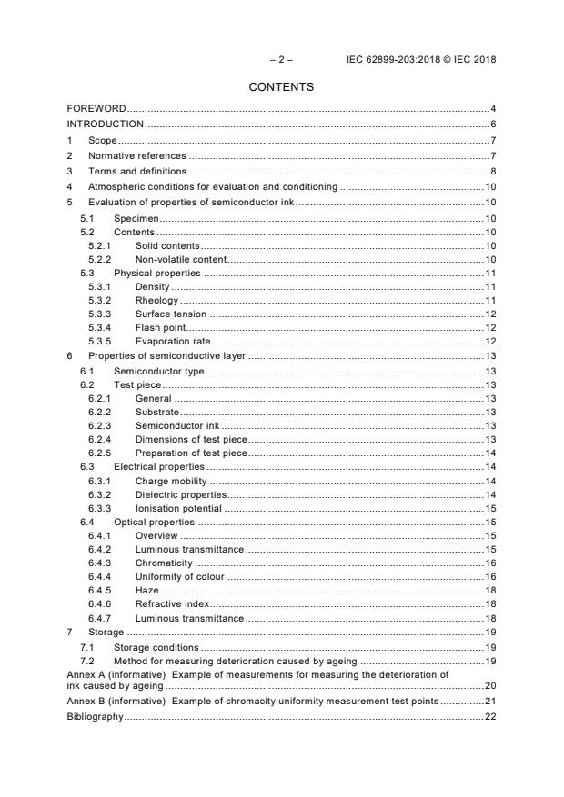
– 2 – IEC 62899-203:2018 © IEC 2018
CONTENTS
FOREWORD . 4
INTRODUCTION . 6
1 Scope . 7
2 Normative references . 7
3 Terms and definitions . 8
4 Atmospheric conditions for evaluation and conditioning . 10
5 Evaluation of properties of semiconductor ink . 10
5.1 Specimen . 10
5.2 Contents . 10
5.2.1 Solid contents . 10
5.2.2 Non-volatile content . 10
5.3 Physical properties . 11
5.3.1 Density . 11
5.3.2 Rheology . 11
5.3.3 Surface tension . 12
5.3.4 Flash point . 12
5.3.5 Evaporation rate . 12
6 Properties of semiconductive layer . 13
6.1 Semiconductor type . 13
6.2 Test piece . 13
6.2.1 General . 13
6.2.2 Substrate . 13
6.2.3 Semiconductor ink . 13
6.2.4 Dimensions of test piece . 13
6.2.5 Preparation of test piece . 14
6.3 Electrical properties . 14
6.3.1 Charge mobility . 14
6.3.2 Dielectric properties . 14
6.3.3 Ionisation potential . 15
6.4 Optical properties . 15
6.4.1 Overview . 15
6.4.2 Luminous transmittance . 15
6.4.3 Chromaticity . 16
6.4.4 Uniformity of colour . 16
6.4.5 Haze . 18
6.4.6 Refractive index . 18
6.4.7 Luminous transmittance . 18
7 Storage . 19
7.1 Storage conditions . 19
7.2 Method for measuring deterioration caused by ageing . 19
Annex A (informative) Example of measurements for measuring the deterioration of
ink caused by ageing . 20
Annex B (informative) Example of chromacity uniformity measurement test points . 21
Bibliography . 22
Figure A.1 – Example of a series of TFT mobility measurements for an ink to evaluate
deterioration over time . 20
Figure B.1 – Chromacity uniformity test point locations . 21
– 4 – IEC 62899-203:2018 © IEC 2018
INTERNATIONAL ELECTROTECHNICAL COMMISSION
____________
PRINTED ELECTRONICS –
Part 203: Materials – Semiconductor ink
FOREWORD
1) The International Electrotechnical Commission (IEC) is a worldwide organization for standardization comprising
all national electrotechnical committees (IEC National Committees). The object of IEC is to promote
international co-operation on all questions concerning standardization in the electrical and electronic fields. To
this end and in addition to other activities, IEC publishes International Standards, Technical Specifications,
Technical Reports, Publicly Available Specifications (PAS) and Guides (hereafter referred to as “IEC
Publication(s)”). Their preparation is entrusted to technical committees; any IEC National Committee interested
in the subject dealt with may participate in this preparatory work. International, governmental and
non-governmental organizations liaising with the IEC also participate in this preparation. IEC collaborates
closely with the International Organization for Standardization (ISO) in accordance with conditions determined
by agreement between the two organizations.
2) The formal decisions or agreements of IEC on technical matters express, as nearly as possible, an international
consensus of opinion on the relevant subjects since each technical committee has representation from all
interested IEC National Committees.
3) IEC Publications have the form of recommendations for international use and are accepted by IEC National
Committees in that sense. While all reasonable efforts are made to ensure that the technical content of IEC
Publications is accurate, IEC cannot be held responsible for the way in which they are used or for any
misinterpretation by any end user.
4) In order to promote international uniformity, IEC National Committees undertake to apply IEC Publications
transparently to the maximum extent possible in their national and regional publications. Any divergence
between any IEC Publication and the corresponding national or regional publication shall be clearly indicated in
the latter.
5) IEC itself does not provide any attestation of conformity. Independent certification bodies provide conformity
assessment services and, in some areas, access to IEC marks of conformity. IEC is not responsible for any
services carried out by independent certification bodies.
6) All users should ensure that they have the latest edition of this publication.
7) No liability shall attach to IEC or its directors, employees, servants or agents including individual experts and
members of its technical committees and IEC National Committees for any personal injury, property damage or
other damage of any nature whatsoever, whether direct or indirect, or for costs (including legal fees) and
expenses arising out of the publication, use of, or reliance upon, this IEC Publication or any other IEC
Publications.
8) Attention is drawn to the Normative references cited in this publication. Use of the referenced publications is
indispensable for the correct application of this publication.
9) Attention is drawn to the possibility that some of the elements of this IEC Publication may be the subject of
patent rights. IEC shall not be held responsible for identifying any or all such patent rights.
International Standard IEC 62899-203 has been prepared by IEC technical committee 119:
Printed Electronics.
The text of this International Standard is based on the following documents:
FDIS Report on voting
119/226/FDIS 119/234/RVD
Full information on the voting for the approval of this International Standard can be found in
the report on voting indicated in the above table.
This document has been drafted in accordance with the ISO/IEC Directives, Part 2.
A list of all parts in the IEC 62899 series, published under the general title Printed electronics,
can be found on the IEC website.
The committee has decided that the contents of this document will remain unchanged until the
stability date indicated on the IEC website under "http://webstore.iec.ch" in the data related to
the specific document. At this date, the document will be
• reconfirmed,
• withdrawn,
• replaced by a revised edition, or
• amended.
A bilingual version of this publication may be issued at a later date.
IMPORTANT – The 'colour inside' logo on the cover page of this publication indicates
that it contains colours which are considered to be useful for the correct
understanding of its contents. Users should therefore print this document using a
colour printer.
– 6 – IEC 62899-203:2018 © IEC 2018
INTRODUCTION
The IEC 62899 series deals mainly with evaluation methods for materials of printed
electronics. The series also includes storage methods, packaging and marking, and
transportation conditions.
The IEC 62899 series is divided into several parts according to each material. Each part is
prepared as a generic specification containing fundamental information for the area of printing
electronics.
The IEC 62899 series consists of the following parts:
Part 1: Terminology
Part 201: Materials – Substrates
Part 202: Materials – Conductive ink
Part 203: Materials – Semiconductor ink
Part 250: Material technologies required in printed electronics for wearable smart devices
Part 301-X: Equipment – Contact printing – Rigid master
Part 302-X: Equipment – Inkjet
Part 303-X: Equipment – Roll-to-roll printing
Part 401: Printability – Overview
Part 402-X: Printability – Measurement of qualities
Part 403-X: Printability – Requirements for reproducibility
Part 502-X: Quality assessment – Organic light emitting diode (OLED) elements
Furthermore, sectional specifications, blank detail specifications, and detail specifications for
each material will be based on these parts.
This part of IEC 62899 is prepared for semiconducting materials used in printed electronics
and contains the test conditions, the evaluation methods and the storage conditions.
PRINTED ELECTRONICS –
Part 203: Materials – Semiconductor ink
1 Scope
This part of IEC 62899 defines terms and specifies standard methods for characterisation and
evaluation.
This document is applicable to semiconductor inks and semiconductive layers that are made
from semiconductor inks.
2 Normative references
The following documents are referred to in the text in such a way that some or all of their
content constitutes requirements of this document. For dated references, only the edition
cited applies. For undated references, the latest edition of the referenced document (including
any amendments) applies.
IEC 62860, Test methods for the characterization of organic transistors and materials
ISO 5-2, Photography and graphic technology – Density measurements – Part 2: Geometric
conditions for transmittance density
ISO 5-3, Photography and graphic technology – Density measurements – Part 3: Spectral
conditions
ISO 124, Latex, rubber – Determination of total solids content
ISO 291, Plastics – Standard atmospheres for conditioning and testing
ISO 304, Surface active agents – Determination of surface tension by drawing up liquid films
ISO 489:1999, Plastics – Determination of refractive index
ISO 758, Liquid chemical products for industrial use – Determination of density at 20°C
ISO 1183-1, Plastics – Methods for determining the density of non-cellular plastics – Part 1:
Immersion method, liquid pyknometer method and titration method
ISO 2555, Plastics – Resins in the liquid state or as emulsions or dispersions – Determination
of apparent viscosity by the Brookfield Test method
ISO 2592, Petroleum and related products – Determination of flash and fire points –
Cleveland closed cup method
ISO 2719, Determination of flash point – Pensky-Martens closed cup method
ISO 2811-1, Paints and varnishes – Determination of density – Part 1: Pyknometer method
– 8 – IEC 62899-203:2018 © IEC 2018
ISO 2811-2, Paints and varnishes – Determination of density – Part 2: Immersed body
(plummet) method
ISO 2884-1, Paints and varnishes – Determination of viscosity using rotary viscometers –
Part 1: Cone-and-plate viscometer operated at a high rate of shear
ISO 3219, Plastics – Polymers/resins in the liquid state or as emulsions or dispersions –
Determination of viscosity using a rotational viscometer with defined shear rate
ISO 3251, Paints, varnishes and plastics – Determination of non-volatile-matter content
ISO 3664, Graphic technology and photography – Viewing conditions
ISO 3679, Determination of flash no-flash and flash point – Rapid equilibrium closed cup
method
ISO 13468-1:1996, Plastics – Determination of the total luminous transmittance of transparent
materials – Part 1: Single-beam instrument
ISO 13468-2:1999, Plastics – Determination of the total luminous transmittance of transparent
materials – Part 2: Double-beam instrument
ISO 13655, Graphic technology – Spectral measurement and colorimetric computation for
graphic arts images
ISO 14488, Particulate materials – Sampling and sample splitting for the determination of
particulate properties
ISO 14782, Plastics – Determination of haze for transparent materials
ISO 15212-1, Oscillation-type density meters – Part 1: Laboratory instruments
3 Terms and definitions
For the purposes of this document, the terms and definitions given in IEC 62860 and the
following apply.
ISO and IEC maintain terminological databases for use in standardization at the following
addresses:
• IEC Electropedia: available at http://www.electropedia.org/
• ISO Online browsing platform: available at http://www.iso.org/obp
NOTE The terms in italic font are those defined in Clause 3.
3.1
semiconductive material
ingredient of a printing or coating material, which itself is electrically semiconductive
3.2
semiconductor ink
liquid in which one or more particles, small molecules or polymers are dissolved or dispersed,
and which becomes an electrically semiconductive layer through solvent removal or post
treatment such as UV, photonic, or thermal processing
3.3
semiconductive layer
film-like semiconductive body of material made of semiconductor ink (3.2), which is printed or
coated on a substrate, followed, as necessary, by using a post treatment such as UV,
photonic, or thermal processing
3.4
semiconductor film
substrate (sheet or roll) with semiconductive layer (3.3)
3.5
solid content
mass fraction of an ingredient which effectively functions as a semiconductive material
dissolved or dispersed in a solvent to form a semiconductor ink (3.2)
Note 1 to entry: In some instances the ink may include insulating materials, sometimes referred to as binders, or
other additives included to improve the film formation during coating or printing.
3.6
non-volatile content
mass fraction of residue obtained by evaporation of the volatile solvent under specific
conditions, in semiconductor ink (3.2)
3.7
dispersion
heterogeneous system in which fine separated materials are distributed uniformly in other
materials
3.8
flash point
lowest liquid temperature at which, under certain standardized conditions, a liquid gives off
vapours in quantity such as to be capable of forming an ignitable vapour/air mixture
[SOURCE: IEC 60050-212:2010, 212-18-05]
3.9
field effect mobility
majority carrier mobility of semiconductive material derived through the transfer curve
measurement of a fabricated TFT device
Note 1 to entry: The field effect mobility is usually derived from either saturation or linear approximations.
Note 2 to entry: Field effect mobility is given in units of cm /V·s.
3.10
thin-film transistor
TFT
switching device made from three electrodes (source, drain and gate) and semiconducting
and insulating layers wherein potentials applied to a gate electrode modulate charge carriers
on the opposite side of the insulating layer situated between the gate and semiconductive
layer
Note 1 to entry: The change in charge density in the semiconductive layer changes its conductivity, and this in
turn allows a modulation in current flow between the source and drain electrodes for a given source-drain potential
difference.
Note 2 to entry: TFTs are found in a wide variety of electronic devices such as integrated circuits and display
backplanes.
– 10 – IEC 62899-203:2018 © IEC 2018
4 Atmospheric conditions for evaluation and conditioning
The standard atmosphere for evaluation (test and measurement) and storage of the specimen
shall be a temperature of (23 ± 2) °C and relative humidity of (50 ± 10) %, conforming to
standard atmosphere class 2 specified in ISO 291. If a polymer substrate is used for a test
piece coated with a semiconductive layer, the standard atmosphere for evaluation shall be a
temperature of (23 ± 1) °C and relative humidity of (50 ± 5) %, conforming to standard
atmosphere class 1 specified in ISO 291.
If conditioning is necessary, the same standard atmosphere as specified above shall apply.
5 Evaluation of properties of semiconductor ink
5.1 Specimen
The specimen for evaluation shall be prepared according to ISO 14488 or an equivalent
method. If necessary, dilution by a compatible solvent may be allowed. For semiconductor
inks, in many cases the properties to be evaluated could be influenced by the choice of
solvent and method of deposition. Consideration of the likely effects of solvent choice and ink
deposition should be made in light of the semiconductor chemistry and/or the ink composition.
5.2 Contents
5.2.1 Solid contents
5.2.1.1 Determination of solid content
Solid content of semiconductive materials and non-semiconductive materials shall be
determined by the theoretical mass fraction (expressed as a percentage) of functional
ingredients to the total ink mass. Functional
...
Questions, Comments and Discussion
Ask us and Technical Secretary will try to provide an answer. You can facilitate discussion about the standard in here.
Loading comments...