IEC 62899-503-3:2021
(Main)Printed electronics - Part 503-3: Quality assessment - Measuring method of contact resistance for the printed thin film transistor - Transfer length method
Printed electronics - Part 503-3: Quality assessment - Measuring method of contact resistance for the printed thin film transistor - Transfer length method
IEC 62899-503-3:2021(E) specifies a measuring method of contact resistance for printed thin film transistors (TFTs) by the transfer length method (TLM). The method requires the fabrication of a test element group (TEG) with varying channel length (L) between source and drain electrodes. The method is intended for quality assessment of TFT electrode contacts and is suited for determining whether the contact resistance lies within a desired range.
General Information
- Status
- Published
- Publication Date
- 23-Aug-2021
- Technical Committee
- TC 119 - Printed Electronics
- Drafting Committee
- WG 5 - TC 119/WG 5
- Current Stage
- PPUB - Publication issued
- Start Date
- 24-Aug-2021
- Completion Date
- 17-Sep-2021
Overview
IEC 62899-503-3:2021 - Printed electronics - Part 503-3 defines a standardized, practical method for measuring contact resistance (Rc) of printed thin film transistors (TFTs) using the transfer length method (TLM). The standard specifies how to fabricate a Test Element Group (TEG) with varying channel lengths, how to perform measurements (using a current meter or SMU), and how to analyze and report results for quality assessment of electrode contacts in printed TFT devices.
Key topics and requirements
- Scope and purpose
- Quality assessment of TFT electrode contacts in printed electronics.
- Suited to determine whether contact resistance lies within a desired range.
- Test Element Group (TEG) preparation
- TEGs must use the same materials, device architecture and (ideally) substrate as the evaluated TFT.
- A set shall include four or more TEGs with different source–drain channel lengths (L).
- Measured L values should be between 0.5 and 5 times the channel length of the evaluated TFT; electrode width (W) should be 0.5–2 times that of the evaluated device.
- Measurement method
- Use the Transfer Length Method (TLM): measure total resistance for different L and extrapolate to L = 0 to extract contact resistance (y-intercept).
- Measurements are performed in the TFT linear regime and require appropriate drain and gate biasing.
- Measurement configurations may use a current meter or a Source Measure Unit (SMU).
- Apparatus, environment and data handling
- Standard specifies measuring apparatus considerations, environmental conditions and storage prior to measurement.
- Data analysis includes normalization of resistance values, plotting total resistance vs. L, and deriving Rc by extrapolation.
- Reporting
- Required reporting items include TEG details, measurement conditions, data analysis method and derived contact resistance.
Practical applications and users
- Who uses it
- Printed electronics manufacturers and suppliers
- Quality, reliability and process engineers
- Test labs and contract manufacturers
- R&D teams developing printed TFTs and materials
- Why it matters
- Enables consistent, repeatable assessment of TFT contact quality across supply chains.
- Helps diagnose process, material or design changes that affect device performance and lifetime.
- Cost-effective method for discrete-device testing without complex equipment.
Related standards
- This document is part of the IEC 62899 series (Printed electronics). Users should consult other parts of the series for complementary test and device specifications and check for the latest editions and related measurement standards.
Keywords: IEC 62899-503-3:2021, printed electronics, thin film transistor, TFT, contact resistance, transfer length method, TLM, Test Element Group, TEG, quality assessment.
Get Certified
Connect with accredited certification bodies for this standard

Intertek Testing Services NA Inc.
Intertek certification services in North America.

UL Solutions
Global safety science company with testing, inspection and certification.

ANCE
Mexican certification and testing association.
Sponsored listings
Frequently Asked Questions
IEC 62899-503-3:2021 is a standard published by the International Electrotechnical Commission (IEC). Its full title is "Printed electronics - Part 503-3: Quality assessment - Measuring method of contact resistance for the printed thin film transistor - Transfer length method". This standard covers: IEC 62899-503-3:2021(E) specifies a measuring method of contact resistance for printed thin film transistors (TFTs) by the transfer length method (TLM). The method requires the fabrication of a test element group (TEG) with varying channel length (L) between source and drain electrodes. The method is intended for quality assessment of TFT electrode contacts and is suited for determining whether the contact resistance lies within a desired range.
IEC 62899-503-3:2021(E) specifies a measuring method of contact resistance for printed thin film transistors (TFTs) by the transfer length method (TLM). The method requires the fabrication of a test element group (TEG) with varying channel length (L) between source and drain electrodes. The method is intended for quality assessment of TFT electrode contacts and is suited for determining whether the contact resistance lies within a desired range.
IEC 62899-503-3:2021 is classified under the following ICS (International Classification for Standards) categories: 29.045 - Semiconducting materials; 31.080.30 - Transistors. The ICS classification helps identify the subject area and facilitates finding related standards.
IEC 62899-503-3:2021 is available in PDF format for immediate download after purchase. The document can be added to your cart and obtained through the secure checkout process. Digital delivery ensures instant access to the complete standard document.
Standards Content (Sample)
IEC 62899-503-3 ®
Edition 1.0 2021-08
INTERNATIONAL
STANDARD
colour
inside
Printed electronics –
Part 503-3: Quality assessment – Measuring method of contact resistance for the
printed thin film transistor – Transfer length method
All rights reserved. Unless otherwise specified, no part of this publication may be reproduced or utilized in any form
or by any means, electronic or mechanical, including photocopying and microfilm, without permission in writing from
either IEC or IEC's member National Committee in the country of the requester. If you have any questions about IEC
copyright or have an enquiry about obtaining additional rights to this publication, please contact the address below or
your local IEC member National Committee for further information.
IEC Central Office Tel.: +41 22 919 02 11
3, rue de Varembé info@iec.ch
CH-1211 Geneva 20 www.iec.ch
Switzerland
About the IEC
The International Electrotechnical Commission (IEC) is the leading global organization that prepares and publishes
International Standards for all electrical, electronic and related technologies.
About IEC publications
The technical content of IEC publications is kept under constant review by the IEC. Please make sure that you have the
latest edition, a corrigendum or an amendment might have been published.
IEC publications search - webstore.iec.ch/advsearchform IEC online collection - oc.iec.ch
The advanced search enables to find IEC publications by a Discover our powerful search engine and read freely all the
variety of criteria (reference number, text, technical publications previews. With a subscription you will always
committee, …). It also gives information on projects, replaced have access to up to date content tailored to your needs.
and withdrawn publications.
Electropedia - www.electropedia.org
IEC Just Published - webstore.iec.ch/justpublished
The world's leading online dictionary on electrotechnology,
Stay up to date on all new IEC publications. Just Published
containing more than 22 000 terminological entries in English
details all new publications released. Available online and
and French, with equivalent terms in 18 additional languages.
once a month by email.
Also known as the International Electrotechnical Vocabulary
(IEV) online.
IEC Customer Service Centre - webstore.iec.ch/csc
If you wish to give us your feedback on this publication or
need further assistance, please contact the Customer Service
Centre: sales@iec.ch.
IEC 62899-503-3 ®
Edition 1.0 2021-08
INTERNATIONAL
STANDARD
colour
inside
Printed electronics –
Part 503-3: Quality assessment – Measuring method of contact resistance for
the printed thin film transistor – Transfer length method
INTERNATIONAL
ELECTROTECHNICAL
COMMISSION
ICS 29.045; 31.080.30 ISBN 978-2-8322-1013-8
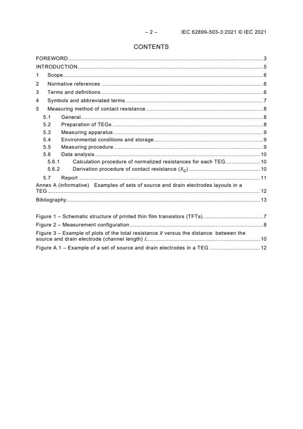
– 2 – IEC 62899-503-3:2021 © IEC 2021
CONTENTS
FOREWORD . 3
INTRODUCTION . 5
1 Scope . 6
2 Normative references . 6
3 Terms and definitions . 6
4 Symbols and abbreviated terms . 7
5 Measuring method of contact resistance . 8
5.1 General . 8
5.2 Preparation of TEGs . 8
5.3 Measuring apparatus . 9
5.4 Environmental conditions and storage . 9
5.5 Measuring procedure . 9
5.6 Data analysis . 10
5.6.1 Calculation procedure of normalized resistances for each TEG. 10
5.6.2 Derivation procedure of contact resistance (R ) . 10
c
5.7 Report . 11
Annex A (informative) Examples of sets of source and drain electrodes layouts in a
TEG . 12
Bibliography . 13
Figure 1 – Schematic structure of printed thin film transistors (TFTs) . 7
Figure 2 – Measurement configuration . 8
Figure 3 – Example of plots of the total resistance R versus the distance between the
source and drain electrode (channel length) L. 10
Figure A.1 – Example of a set of source and drain electrodes in a TEG . 12
INTERNATIONAL ELECTROTECHNICAL COMMISSION
____________
PRINTED ELECTRONICS –
Part 503-3: Quality assessment – Measuring method of contact
resistance for the printed thin film transistor – Transfer length method
FOREWORD
1) The International Electrotechnical Commission (IEC) is a worldwide organization for standardization comprising
all national electrotechnical committees (IEC National Committees). The object of IEC is to promote international
co-operation on all questions concerning standardization in the electrical and electronic fields. To this end and
in addition to other activities, IEC publishes International Standards, Technical Specifications, Technical Reports,
Publicly Available Specifications (PAS) and Guides (hereafter referred to as “IEC Publication(s)”). Their
preparation is entrusted to technical committees; any IEC National Committee interested in the subject dealt with
may participate in this preparatory work. International, governmental and non-governmental organizations liaising
with the IEC also participate in this preparation. IEC collaborates closely with the International Organization for
Standardization (ISO) in accordance with conditions determined by agreement between the two organizations.
2) The formal decisions or agreements of IEC on technical matters express, as nearly as possible, an international
consensus of opinion on the relevant subjects since each technical committee has representation from all
interested IEC National Committees.
3) IEC Publications have the form of recommendations for international use and are accepted by IEC National
Committees in that sense. While all reasonable efforts are made to ensure that the technical content of IEC
Publications is accurate, IEC cannot be held responsible for the way in which they are used or for any
misinterpretation by any end user.
4) In order to promote international uniformity, IEC National Committees undertake to apply IEC Publications
transparently to the maximum extent possible in their national and regional publications. Any divergence between
any IEC Publication and the corresponding national or regional publication shall be clearly indicated in the latter.
5) IEC itself does not provide any attestation of conformity. Independent certification bodies provide conformity
assessment services and, in some areas, access to IEC marks of conformity. IEC is not responsible for any
services carried out by independent certification bodies.
6) All users should ensure that they have the latest edition of this publication.
7) No liability shall attach to IEC or its directors, employees, servants or agents including individual experts and
members of its technical committees and IEC National Committees for any personal injury, property damage or
other damage of any nature whatsoever, whether direct or indirect, or for costs (including legal fees) and
expenses arising out of the publication, use of, or reliance upon, this IEC Publication or any other IEC
Publications.
8) Attention is drawn to the Normative references cited in this publication. Use of the referenced publications is
indispensable for the correct application of this publication.
9) Attention is drawn to the possibility that some of the elements of this IEC Publication may be the subject of patent
rights. IEC shall not be held responsible for identifying any or all such patent rights.
International Standard IEC 62899-503-3 has been prepared by IEC technical committee 119:
Printed Electronics.
The text of this International Standard is based on the following documents:
FDIS Report on voting
119/359/FDIS 119/368/RVD
Full information on the voting for its approval can be found in the report on voting indicated in
the above table.
The language used for the development of this International Standard is English.
– 4 – IEC 62899-503-3:2021 © IEC 2021
This document was drafted in accordance with ISO/IEC Directives, Part 2, and developed in
accordance with ISO/IEC Directives, Part 1 and ISO/IEC Directives, IEC Supplement, available
at www.iec.ch/members_experts/refdocs. The main document types developed by IEC are
described in greater detail at www.iec.ch/standardsdev/publications.
A list of all parts in the IEC 62899 series, published under the general title Printed electronics,
can be found on the IEC website.
The committee has decided that the contents of this document will remain unchanged until the
stability date indicated on the IEC website under webstore.iec.ch in the data related to the
specific document. At this date, the document will be
• reconfirmed,
• withdrawn,
• replaced by a revised edition, or
• amended.
IMPORTANT – The "colour inside" logo on the cover page of this document indicates that it
contains colours which are considered to be useful for the correct understanding of its
contents. Users should therefore print this document using a colour printer.
INTRODUCTION
In a thin film transistor (TFT), contact resistance occurs at the contacting interfaces at the gate,
source and drain electrodes, and the TFT semiconductor layer. While contact resistance is
negligible at the gate electrode, it reduces the effective voltage applied to the source and drain
electrodes. Therefore, the evaluation of the contact resistance can provide important insights
related to the performance characteristics of printed TFTs. Especially for printed electronics,
the contact resistance varies with the employed materials, printing processes and the time
series variation because the interface is made of simple contact obtained by additive
manufacturing instead of a junction obtained by vacuum deposition and etching processes.
Thus, the performance of printed TFTs is greatly influenced by the value of contact resistance.
A change of the contact resistance is therefore considered to be a key factor for a proper
interpretation of performance, lifetime, and reliability of a printed TFT.
To determine the contact resistance, several techniques, including but not limited to two-
terminal contact method, four-terminal contact method, six-terminal contact method, transfer
length method, and scanning probe potentiometer technique can be used. The transfer length
method (TLM) in particular has a practical advantage because the supplier can test discrete
devices, which have the same structure as the original printed TFT, on a common substrate
simultaneously. Furthermore, the TLM is cost-effective because the user can meas
...
Questions, Comments and Discussion
Ask us and Technical Secretary will try to provide an answer. You can facilitate discussion about the standard in here.
Loading comments...