ISO 8181:2023
(Main)Atomic layer deposition — Vocabulary
Atomic layer deposition — Vocabulary
This document defines general terms and film growth processes for atomic layer deposition (ALD). ALD technique is classified into conventional time separated ALD and spatial ALD according to the separation between sequential surface reactions of precursors on substrate. Besides planar substrate, ALD can be used for coating on micro-nano particles, which is developed as powder ALD. Some energy enhanced ALD techniques are also included. This document specifies the processes of different ALD methods. This document applies to the process of ALD. This document does not apply to the deposited materials or specific nanostructures. This document applies to industrial production, scientific research, teaching, publishing and scientific and technological communications related to ALD.
Dépôt de couches atomiques — Vocabulaire
General Information
- Status
- Published
- Publication Date
- 15-Oct-2023
- Technical Committee
- ISO/TC 107 - Metallic and other inorganic coatings
- Drafting Committee
- ISO/TC 107 - Metallic and other inorganic coatings
- Current Stage
- 6060 - International Standard published
- Start Date
- 16-Oct-2023
- Due Date
- 05-Aug-2024
- Completion Date
- 16-Oct-2023
Overview
ISO 8181:2023, titled Atomic Layer Deposition - Vocabulary, is an international standard developed by ISO’s Technical Committee ISO/TC 107. This standard precisely defines general terms and film growth processes related to Atomic Layer Deposition (ALD). ALD is a cutting-edge thin film deposition technique based on sequential and self-limiting chemical reactions of gas phase precursors on substrates, allowing for atomic scale thickness control.
The document covers various ALD classifications such as conventional time separated ALD, spatial ALD, and powder ALD for micro-nano particles. It also includes energy-enhanced ALD methods like plasma-enhanced, photo-assisted, and catalytic ALD. Importantly, ISO 8181:2023 focuses on the ALD processes themselves, not on the materials deposited or specific nanostructures.
This vocabulary standard is essential for ensuring consistent terminology in scientific research, industrial production, education, and technology communications related to ALD across global settings.
Key Topics
ALD Process Terms
Fundamental definitions such as precursor, self-limiting reaction, half chemical reaction, and growth rate help clearly describe how ALD cycles produce uniform thin films.Film Growth Stages
Key terms defining ALD film formation include nucleation, nucleation site, island stage, network stage, and continuous stage, detailing how film morphology evolves during deposition.ALD Classifications
ALD is classified by process separation into:- Time separated ALD - where sequential surface reactions are separated in time.
- Spatial ALD - where the substrate alternately encounters different precursor zones spatially.
Substrate types classify ALD as planar or powder ALD. Reaction activation methods divide ALD further into thermal, plasma-enhanced, photo-assisted, and catalytic ALD.
Specialized Terms
Terms such as inert gas, carrier gas, precursor exposure, inert gas purge, and vacuum-related parameters aid in describing ALD process environments.Selectivity and Energy
Vocabulary includes selective atomic layer deposition, selectivity, facet selectivity, and various energy terms like precursor bonding energy and activation energy crucial for understanding reaction mechanisms.
Applications
ISO 8181:2023 supports professionals involved in:
Industrial Production
Helping manufacturers apply standardized ALD terminology for coating uniform thin films on electronics, photovoltaics, and flexible substrates.Scientific Research
Guiding researchers in communicating precise ALD process details and advances in micro-nano particle coatings and energy-enhanced ALD.Education & Publishing
Offering clear ALD vocabularies for curriculum development, technical documentation, and academic journals worldwide.Technology Communication
Facilitating consistent, global exchanges in conferences, patents, and cross-industry collaborations concerning ALD advancements.
Related Standards
- ISO/TS 80004-8:2020 – Defines vocabularies on nanomanufacturing processes related to ALD.
- ISO 20523:2017 – Covers carbon-based film classification, complementing ALD thin film standards.
- ISO 18115-1:2023 – Provides general surface chemical analysis terminology used in ALD film characterization.
Summary
ISO 8181:2023 is a foundational vocabulary standard for Atomic Layer Deposition, covering critical process definitions, classification schemes, and operational terminology. By adopting this standard, industries and researchers ensure uniform understanding and communication of ALD techniques-enabling precise control of ultra-thin films and expanding ALD applications from electronics to biomedicine. This standard is indispensable for advancing innovation, quality control, and international collaboration in the growing field of atomic layer deposition.
Get Certified
Connect with accredited certification bodies for this standard

National Aerospace and Defense Contractors Accreditation Program (NADCAP)
Global cooperative program for special process quality in aerospace.

CARES (UK Certification Authority for Reinforcing Steels)
UK certification for reinforcing steels and construction.

DVS-ZERT GmbH
German welding certification society.
Sponsored listings
Frequently Asked Questions
ISO 8181:2023 is a standard published by the International Organization for Standardization (ISO). Its full title is "Atomic layer deposition — Vocabulary". This standard covers: This document defines general terms and film growth processes for atomic layer deposition (ALD). ALD technique is classified into conventional time separated ALD and spatial ALD according to the separation between sequential surface reactions of precursors on substrate. Besides planar substrate, ALD can be used for coating on micro-nano particles, which is developed as powder ALD. Some energy enhanced ALD techniques are also included. This document specifies the processes of different ALD methods. This document applies to the process of ALD. This document does not apply to the deposited materials or specific nanostructures. This document applies to industrial production, scientific research, teaching, publishing and scientific and technological communications related to ALD.
This document defines general terms and film growth processes for atomic layer deposition (ALD). ALD technique is classified into conventional time separated ALD and spatial ALD according to the separation between sequential surface reactions of precursors on substrate. Besides planar substrate, ALD can be used for coating on micro-nano particles, which is developed as powder ALD. Some energy enhanced ALD techniques are also included. This document specifies the processes of different ALD methods. This document applies to the process of ALD. This document does not apply to the deposited materials or specific nanostructures. This document applies to industrial production, scientific research, teaching, publishing and scientific and technological communications related to ALD.
ISO 8181:2023 is classified under the following ICS (International Classification for Standards) categories: 01.040.25 - Manufacturing engineering (Vocabularies); 25.220.01 - Surface treatment and coating in general. The ICS classification helps identify the subject area and facilitates finding related standards.
ISO 8181:2023 is available in PDF format for immediate download after purchase. The document can be added to your cart and obtained through the secure checkout process. Digital delivery ensures instant access to the complete standard document.
Standards Content (Sample)
INTERNATIONAL ISO
STANDARD 8181
First edition
2023-10
Atomic layer deposition — Vocabulary
Dépôt de couches atomiques — Vocabulaire
Reference number
© ISO 2023
All rights reserved. Unless otherwise specified, or required in the context of its implementation, no part of this publication may
be reproduced or utilized otherwise in any form or by any means, electronic or mechanical, including photocopying, or posting on
the internet or an intranet, without prior written permission. Permission can be requested from either ISO at the address below
or ISO’s member body in the country of the requester.
ISO copyright office
CP 401 • Ch. de Blandonnet 8
CH-1214 Vernier, Geneva
Phone: +41 22 749 01 11
Email: copyright@iso.org
Website: www.iso.org
Published in Switzerland
ii
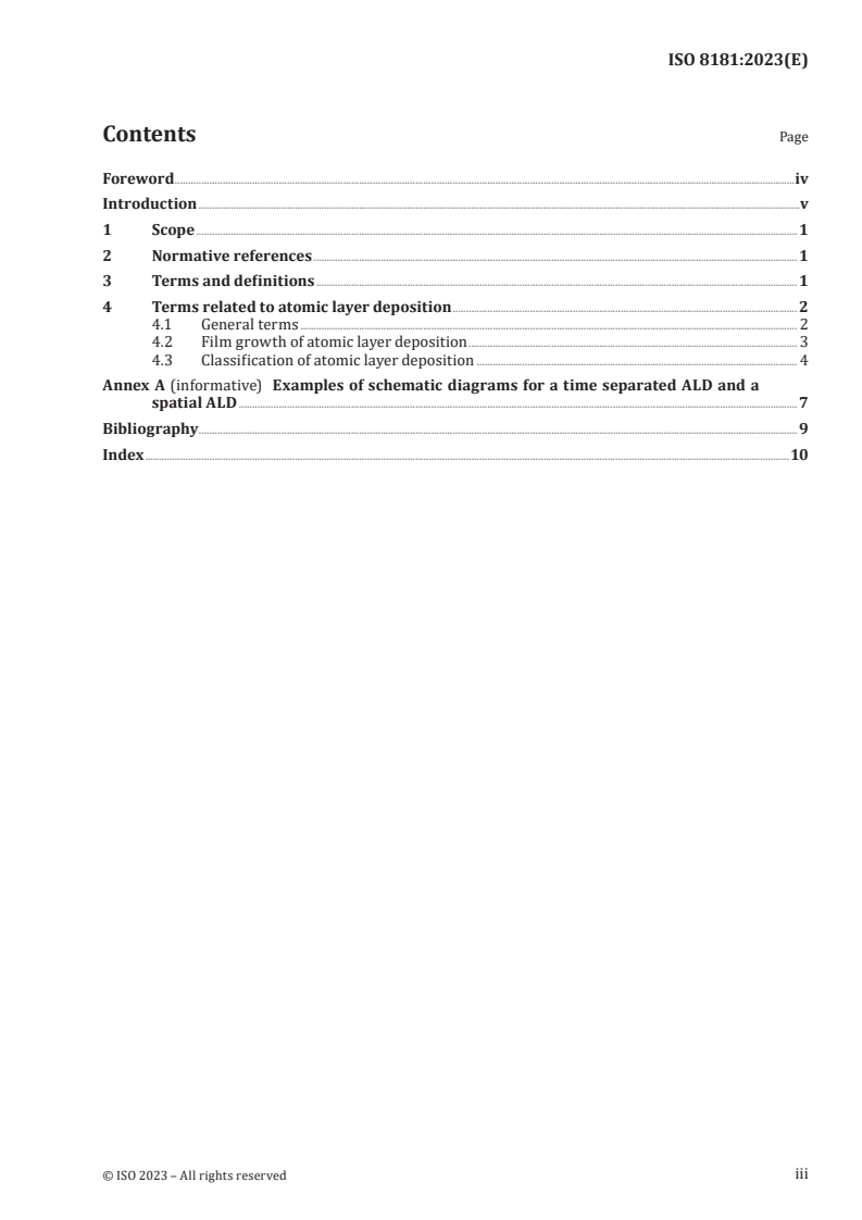
Contents Page
Foreword .iv
Introduction .v
1 Scope . 1
2 Normative references . 1
3 Terms and definitions . 1
4 Terms related to atomic layer deposition . 2
4.1 General terms . 2
4.2 Film growth of atomic layer deposition . 3
4.3 Classification of atomic layer deposition . 4
Annex A (informative) Examples of schematic diagrams for a time separated ALD and a
spatial ALD . 7
Bibliography . 9
Index .10
iii
Foreword
ISO (the International Organization for Standardization) is a worldwide federation of national standards
bodies (ISO member bodies). The work of preparing International Standards is normally carried out
through ISO technical committees. Each member body interested in a subject for which a technical
committee has been established has the right to be represented on that committee. International
organizations, governmental and non-governmental, in liaison with ISO, also take part in the work.
ISO collaborates closely with the International Electrotechnical Commission (IEC) on all matters of
electrotechnical standardization.
The procedures used to develop this document and those intended for its further maintenance are
described in the ISO/IEC Directives, Part 1. In particular, the different approval criteria needed for the
different types of ISO document should be noted. This document was drafted in accordance with the
editorial rules of the ISO/IEC Directives, Part 2 (see www.iso.org/directives).
ISO draws attention to the possibility that the implementation of this document may involve the use
of (a) patent(s). ISO takes no position concerning the evidence, validity or applicability of any claimed
patent rights in respect thereof. As of the date of publication of this document, ISO had not received
notice of (a) patent(s) which may be required to implement this document. However, implementers are
cautioned that this may not represent the latest information, which may be obtained from the patent
database available at www.iso.org/patents. ISO shall not be held responsible for identifying any or all
such patent rights.
Any trade name used in this document is information given for the convenience of users and does not
constitute an endorsement.
For an explanation of the voluntary nature of standards, the meaning of ISO specific terms and
expressions related to conformity assessment, as well as information about ISO's adherence to
the World Trade Organization (WTO) principles in the Technical Barriers to Trade (TBT), see
www.iso.org/iso/foreword.html.
This document was prepared by Technical Committee ISO/TC 107, Metallic and other inorganic coatings.
Any feedback or questions on this document should be directed to the user’s national standards body. A
complete listing of these bodies can be found at www.iso.org/members.html.
iv
Introduction
Atomic layer deposition (ALD) is a thin film deposition technique based on the sequential and self-
limiting surface reactions of gas phase precursors on substrate. ALD is able to meet the needs for
precise thickness control by changing the deposition cycles. ALD films are uniform and remain
extremely conformal to the original substrate since the chemical adsorption and reaction of precursors
on substrate is self-limiting during each ALD cycle. ALD can also be extendible to large substrates,
flexible substrates and large amounts of micro-nano particles. Therefore, the applications of ALD
have covered microelectronics, photovoltaics and displays, as well as many emerging fields, including
renewable energy, catalysis and biomedicine.
The aim of this document is to provide the systematic terminologies about ALD technique. This enables
global professional communications in both industry and academia.
v
INTERNATIONAL STANDARD ISO 8181:2023(E)
Atomic layer deposition — Vocabulary
1 Scope
This document defines general terms and film growth processes for atomic layer deposition (ALD).
ALD technique is classified into conventional time separated ALD and spatial ALD according to the
separation between sequential surface reactions of precursors on substrate. Besides planar substrate,
ALD can be used for coating on micro-nano particles, which is developed as powder ALD. Some energy
enhanced ALD techniques are also included. This document specifies the processes of different ALD
methods.
This document applies to the process of ALD. This document does not apply to the deposited materials
or specific nanostructures.
This document applies to industrial production, scientific research, teaching, publishing and scientific
and technological communications related to ALD.
2 Normative references
There are no normative references in this document.
3 Terms and definitions
ISO and IEC maintain terminology databases for use in standardization at the following addresses:
— ISO Online browsing platform: available at https:// www .iso .org/ obp
— IEC Electropedia: available at https:// www .electropedia .org/
3.1
atomic layer deposition
process of fabricating uniform and conformal films through the cyclic deposition of material by
alternate self-saturating surface absorption and chemical reactions that enable thickness control at the
atomic scale
Note 1 to entry: This process often involves the use of at least two sequential reactions to complete a cycle that
can be repeated several times to establish a desired thickness.
[SOURCE: ISO/TS 80004-8:2020, 8.2.2, modified — "through self-terminating surface reactions"
has been replaced by "by alternate self-saturating surface absorption and chemical reactions" in the
definition.]
3.2
substrate
workpiece upon which deposition is to take place
[SOURCE: ISO 20523:2017, 3.1]
3.3
thin film
layer of material, typically less than 100 nm in thickness, deposited or grown on a substrate
Note 1 to entry: Films thinner than 10 nm are often called ultrathin films.
[SOURCE: ISO 18115-1:2023, 5.13]
4 Terms related to atomic layer deposition
4.1 General terms
4.1.1
precursor
reaction source used in atomic layer deposition process
Note 1 to entry: Metal films can be deposited by reducing precursors and removing ligands linked to metal atoms
in atomic layer deposition process.
Note 2 to entry: Inorganic non-metals film can be deposited by oxidizing or reducing precursors and removing
ligands linked to metal or non-metal atoms in atomic layer deposition process.
4.1.2
self-limiting reaction
reaction between precursor B and substrate with the chemically adsorbed precursor A, which
automatically stops after the substrate is terminated by the remained ligands of precursor B
Note 1 to entry: During a typical atomic layer deposition process, precursor A is chemically adsorbed on the
surface of a substrate, then precursor B will react with precursor A until adsorbed precursor A is completely
consumed.
4.1.3
half chemical reaction
chemical reaction between one kind of precursor and substrate, which makes the substrate expose the
remaining ligands of the precursor
4.1.4
growth rate
film thickness growth in each atomic layer deposition cycle
Note 1 to entry: Growth rate can be measured in situ by a spectroscopic ellipsometer.
4.1.5
atomic layer deposition window
temperature range in which atomic layer deposition reaction can occur
Note 1 t
...


Questions, Comments and Discussion
Ask us and Technical Secretary will try to provide an answer. You can facilitate discussion about the standard in here.
Loading comments...