IEC 62047-46:2025
(Main)Semiconductor devices - Micro-electromechanical devices - Part 46: Silicon based MEMS fabrication technology - Measurement method of tensile strength of nanoscale thickness membrane
Semiconductor devices - Micro-electromechanical devices - Part 46: Silicon based MEMS fabrication technology - Measurement method of tensile strength of nanoscale thickness membrane
IEC 62047-46:2025 specifies the requirements and testing method to measure the tensile strength of membrane with nanoscale thickness (length from 100 μm to 5 000 μm, width from 100 μm to 1 000 μm, thickness from 50 nm to 500 nm) which is fabricated by micromachining technology used in silicon-based micro-electromechanical system (MEMS).
This document is applicable to in-situ tensile strength measurement of nanoscale thickness membrane manufactured by microelectronics technology and related micromachining technology.
With the devices scaling, the tensile strength degradation, induced by defects and contaminations, becomes severer. This document specifies an in-situ testing method of the tensile strength of membrane with nanoscale thickness based on a MEMS technique. This document does not need intricate instruments (such as scanning probe microscopy and nanoindenter) and special test specimens.
Since in-situ on-chip tester in this document and device are fabricated with the same process on the same wafer, this document can give some practical reference for the design part.
General Information
- Status
- Published
- Publication Date
- 22-Apr-2025
- Technical Committee
- SC 47F - Micro-electromechanical systems
- Current Stage
- PPUB - Publication issued
- Start Date
- 23-Apr-2025
- Completion Date
- 09-May-2025
Overview
IEC 62047-46:2025 defines an in‑situ tensile strength measurement method for silicon-based MEMS membranes with nanoscale thickness. The standard covers membranes fabricated by micromachining and microelectronics technology whose dimensions fall in the ranges: length 100 µm–5 000 µm, width 100 µm–1 000 µm, thickness 50 nm–500 nm. It specifies design, fabrication and test‑execution requirements for an on‑chip tester that enables tensile testing without specialized instruments such as AFM or nanoindenters.
Key topics and requirements
- Scope and applicability
- In‑situ tensile strength measurement of nanoscale thickness membranes produced in the same process and wafer as MEMS devices.
- In‑situ on‑chip tester design
- Tester integrates testing structure and testing device on one chip (on‑chip tester).
- Overlap between testing structure and testing device must exceed 30 µm to prevent detachment during test.
- End geometry must ensure fracture occurs in the mid‑section of the membrane.
- Folded beam stiffness should be at least two orders of magnitude lower than the testing structure stiffness so measured force approximates tensile force.
- Fixed column and ring structures must form a process‑limited fixed hinge to maintain axial tensile loading.
- Deflection ruler must be readable with optical microscopy (design guidance in Annex A).
- Fabrication
- Tester and device must share the same silicon process; in‑situ tester made of crystalline silicon (examples include bulk silicon processes and silicon–glass anodic bonding).
- Testing environment and method
- Tests are performed in the device’s manufacturing environment (actual MEMS chip environment).
- The method monitors device deformation under a driving load using microscopy; tensile strength is computed from the maximum observed force divided by original cross‑sectional area.
- Measurement resolution
- Aspect ratios of elastic beams and testing structures must be selected to achieve a stress measurement resolution of ≤100 MPa.
Applications and users
- MEMS device designers seeking process‑relevant mechanical property data for design validation.
- Process engineers in semiconductor fabs for monitoring tensile strength degradation due to defects or contamination.
- R&D teams developing silicon‑based micro‑electromechanical devices who need on‑wafer, non‑intrusive tensile testing.
- Test laboratories that implement wafer‑level mechanical characterization without AFM/nanoindenter equipment.
Related standards
- Part of the IEC 62047 series (Micro‑electromechanical devices). See IEC 62047‑45:2025 for related terminology and testing structure/device definitions.
Keywords: IEC 62047-46:2025, tensile strength, nanoscale thickness membrane, in‑situ on‑chip tester, silicon-based MEMS fabrication, micromachining, tensile testing.
IEC 62047-46:2025 - Semiconductor devices - Micro-electromechanical devices - Part 46: Silicon based MEMS fabrication technology - Measurement method of tensile strength of nanoscale thickness membrane Released:23. 04. 2025 Isbn:9782832703502
Frequently Asked Questions
IEC 62047-46:2025 is a standard published by the International Electrotechnical Commission (IEC). Its full title is "Semiconductor devices - Micro-electromechanical devices - Part 46: Silicon based MEMS fabrication technology - Measurement method of tensile strength of nanoscale thickness membrane". This standard covers: IEC 62047-46:2025 specifies the requirements and testing method to measure the tensile strength of membrane with nanoscale thickness (length from 100 μm to 5 000 μm, width from 100 μm to 1 000 μm, thickness from 50 nm to 500 nm) which is fabricated by micromachining technology used in silicon-based micro-electromechanical system (MEMS). This document is applicable to in-situ tensile strength measurement of nanoscale thickness membrane manufactured by microelectronics technology and related micromachining technology. With the devices scaling, the tensile strength degradation, induced by defects and contaminations, becomes severer. This document specifies an in-situ testing method of the tensile strength of membrane with nanoscale thickness based on a MEMS technique. This document does not need intricate instruments (such as scanning probe microscopy and nanoindenter) and special test specimens. Since in-situ on-chip tester in this document and device are fabricated with the same process on the same wafer, this document can give some practical reference for the design part.
IEC 62047-46:2025 specifies the requirements and testing method to measure the tensile strength of membrane with nanoscale thickness (length from 100 μm to 5 000 μm, width from 100 μm to 1 000 μm, thickness from 50 nm to 500 nm) which is fabricated by micromachining technology used in silicon-based micro-electromechanical system (MEMS). This document is applicable to in-situ tensile strength measurement of nanoscale thickness membrane manufactured by microelectronics technology and related micromachining technology. With the devices scaling, the tensile strength degradation, induced by defects and contaminations, becomes severer. This document specifies an in-situ testing method of the tensile strength of membrane with nanoscale thickness based on a MEMS technique. This document does not need intricate instruments (such as scanning probe microscopy and nanoindenter) and special test specimens. Since in-situ on-chip tester in this document and device are fabricated with the same process on the same wafer, this document can give some practical reference for the design part.
IEC 62047-46:2025 is classified under the following ICS (International Classification for Standards) categories: 31.080.99 - Other semiconductor devices. The ICS classification helps identify the subject area and facilitates finding related standards.
IEC 62047-46:2025 is available in PDF format for immediate download after purchase. The document can be added to your cart and obtained through the secure checkout process. Digital delivery ensures instant access to the complete standard document.
Standards Content (Sample)
IEC 62047-46 ®
Edition 1.0 2025-04
INTERNATIONAL
STANDARD
Semiconductor devices – Micro-electromechanical devices –
Part 46: Silicon based MEMS fabrication technology – Measurement method of
tensile strength of nanoscale thickness membrane
All rights reserved. Unless otherwise specified, no part of this publication may be reproduced or utilized in any form
or by any means, electronic or mechanical, including photocopying and microfilm, without permission in writing from
either IEC or IEC's member National Committee in the country of the requester. If you have any questions about IEC
copyright or have an enquiry about obtaining additional rights to this publication, please contact the address below or
your local IEC member National Committee for further information.
IEC Secretariat Tel.: +41 22 919 02 11
3, rue de Varembé info@iec.ch
CH-1211 Geneva 20 www.iec.ch
Switzerland
About the IEC
The International Electrotechnical Commission (IEC) is the leading global organization that prepares and publishes
International Standards for all electrical, electronic and related technologies.
About IEC publications
The technical content of IEC publications is kept under constant review by the IEC. Please make sure that you have the
latest edition, a corrigendum or an amendment might have been published.
IEC publications search - webstore.iec.ch/advsearchform IEC Products & Services Portal - products.iec.ch
The advanced search enables to find IEC publications by a Discover our powerful search engine and read freely all the
variety of criteria (reference number, text, technical publications previews, graphical symbols and the glossary.
committee, …). It also gives information on projects, replaced With a subscription you will always have access to up to date
and withdrawn publications. content tailored to your needs.
IEC Just Published - webstore.iec.ch/justpublished
Electropedia - www.electropedia.org
Stay up to date on all new IEC publications. Just Published
The world's leading online dictionary on electrotechnology,
details all new publications released. Available online and once
containing more than 22 500 terminological entries in English
a month by email.
and French, with equivalent terms in 25 additional languages.
Also known as the International Electrotechnical Vocabulary
IEC Customer Service Centre - webstore.iec.ch/csc
(IEV) online.
If you wish to give us your feedback on this publication or need
further assistance, please contact the Customer Service
Centre: sales@iec.ch.
IEC 62047-46 ®
Edition 1.0 2025-04
INTERNATIONAL
STANDARD
Semiconductor devices – Micro-electromechanical devices –
Part 46: Silicon based MEMS fabrication technology – Measurement method of
tensile strength of nanoscale thickness membrane
INTERNATIONAL
ELECTROTECHNICAL
COMMISSION
ICS 31.080.99 ISBN 978-2-8327-0350-2
– 2 – IEC 62047-46:2025 © IEC 2025
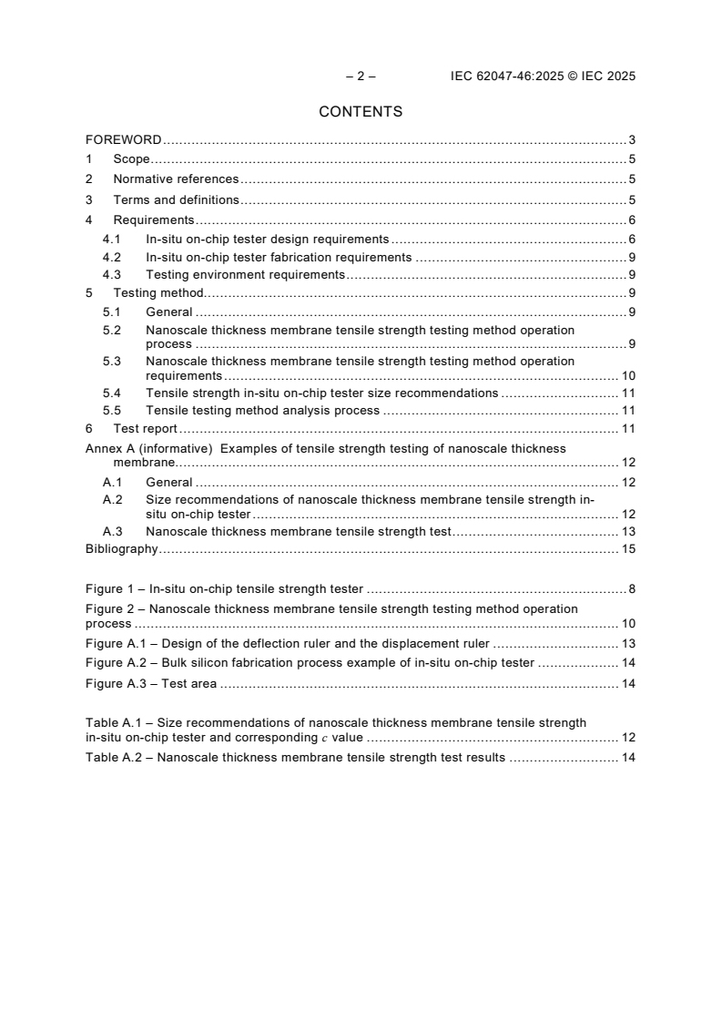
CONTENTS
FOREWORD . 3
1 Scope . 5
2 Normative references . 5
3 Terms and definitions . 5
4 Requirements . 6
4.1 In-situ on-chip tester design requirements . 6
4.2 In-situ on-chip tester fabrication requirements . 9
4.3 Testing environment requirements . 9
5 Testing method. 9
5.1 General . 9
5.2 Nanoscale thickness membrane tensile strength testing method operation
process . 9
5.3 Nanoscale thickness membrane tensile strength testing method operation
requirements . 10
5.4 Tensile strength in-situ on-chip tester size recommendations . 11
5.5 Tensile testing method analysis process . 11
6 Test report . 11
Annex A (informative) Examples of tensile strength testing of nanoscale thickness
membrane. 12
A.1 General . 12
A.2 Size recommendations of nanoscale thickness membrane tensile strength in-
situ on-chip tester . 12
A.3 Nanoscale thickness membrane tensile strength test . 13
Bibliography . 15
Figure 1 – In-situ on-chip tensile strength tester . 8
Figure 2 – Nanoscale thickness membrane tensile strength testing method operation
process . 10
Figure A.1 – Design of the deflection ruler and the displacement ruler . 13
Figure A.2 – Bulk silicon fabrication process example of in-situ on-chip tester . 14
Figure A.3 – Test area . 14
Table A.1 – Size recommendations of nanoscale thickness membrane tensile strength
in-situ on-chip tester and corresponding c value . 12
Table A.2 – Nanoscale thickness membrane tensile strength test results . 14
INTERNATIONAL ELECTROTECHNICAL COMMISSION
____________
SEMICONDUCTOR DEVICES –
MICRO-ELECTROMECHANICAL DEVICES –
Part 46: Silicon based MEMS fabrication technology –
Measurement method of tensile strength
of nanoscale thickness membrane
FOREWORD
1) The International Electrotechnical Commission (IEC) is a worldwide organization for standardization comprising
all national electrotechnical committees (IEC National Committees). The object of IEC is to promote international
co-operation on all questions concerning standardization in the electrical and electronic fields. To this end and
in addition to other activities, IEC publishes International Standards, Technical Specifications, Technical Reports,
Publicly Available Specifications (PAS) and Guides (hereafter referred to as "IEC Publication(s)"). Their
preparation is entrusted to technical committees; any IEC National Committee interested in the subject dealt with
may participate in this preparatory work. International, governmental and non-governmental organizations liaising
with the IEC also participate in this preparation. IEC collaborates closely with the International Organization for
Standardization (ISO) in accordance with conditions determined by agreement between the two organizations.
2) The formal decisions or agreements of IEC on technical matters express, as nearly as possible, an international
consensus of opinion on the relevant subjects since each technical committee has representation from all
interested IEC National Committees.
3) IEC Publications have the form of recommendations for international use and are accepted by IEC National
Committees in that sense. While all reasonable efforts are made to ensure that the technical content of IEC
Publications is accurate, IEC cannot be held responsible for the way in which they are used or for any
misinterpretation by any end user.
4) In order to promote international uniformity, IEC National Committees undertake to apply IEC Publications
transparently to the maximum extent possible in their national and regional publications. Any divergence between
any IEC Publication and the corresponding national or regional publication shall be clearly indicated in the latter.
5) IEC itself does not provide any attestation of conformity. Independent certification bodies provide conformity
assessment services and, in some areas, access to IEC marks of conformity. IEC is not responsible for any
services carried out by independent certification bodies.
6) All users should ensure that they have the latest edition of this publication.
7) No liability shall attach to IEC or its directors, employees, servants or agents including individual experts and
members of its technical committees and IEC National Committees for any personal injury, property damage or
other damage of any nature whatsoever, whether direct or indirect, or for costs (including legal fees) and
expenses arising out of the publication, use of, or reliance upon, this IEC Publication or any other IEC
Publications.
8) Attention is drawn to the Normative references cited in this publication. Use of the referenced publications is
indispensable for the correct application of this publication.
9) IEC draws attention to the possibility that the implementation of this document may involve the use of (a)
patent(s). IEC takes no position concerning the evidence, validity or applicability of any claimed patent rights in
respect thereof. As of the date of publication of this document, IEC had not received notice of (a) patent(s), which
may be required to implement this document. However, implementers are cautioned that this may not represent
the latest information, which may be obtained from the patent database available at https://patents.iec.ch. IEC
shall not be held responsible for identifying any or all such patent rights.
IEC 62047-46 has been prepared by subcommittee 47F: Micro electromechanical systems, of
IEC technical committee 47: Semiconductor devices. It is an International Standard.
The text of this International Standard is based on the following documents:
Draft Report on voting
47F/500/FDIS 47F/507/RVD
Full information on the voting for its approval can be found in the report on voting indicated in
the above table.
– 4 – IEC 62047-46:2025 © IEC 2025
The language used for the development of this International Standard is English.
This document was drafted in accordance with ISO/IEC Directives, Part 2, and developed in
accordance with ISO/IEC Directives, Part 1 and ISO/IEC Directives, IEC Supplement, available
at www.iec.ch/members_experts/refdocs. The main document types developed by IEC are
described in greater detail at www.iec.ch/publications.
A list of all parts in the IEC 62047 series, published under the general title Semiconductor
devices – Micro-electromechanical devices, can be found on the IEC website.
The committee has decided that the contents of this document will remain unchanged until the
stability date indicated on the IEC website under webstore.iec.ch in the data related to the
specific document. At this date, the document will be
• reconfirmed,
• withdrawn, or
• revised.
SEMICONDUCTOR DEVICES –
MICRO-ELECTROMECHANICAL DEVICES –
Part 46: Silicon based MEMS fabrication technology –
Measurement method of tensile strength
of nanoscale thickness membrane
1 Scope
This part of IEC 62047 specifies the requirements and testing method to measure the tensile
strength of membrane with nanoscale thickness (length from 100 μm to 5 000 μm, width from
100 μm to 1 000 μm, thickness from 50 nm to 500 nm) which is fabricated by micromachining
technology used in silicon-based micro-electromechanical system (MEMS).
This document is applicable to in-situ tensile strength measurement of nanoscale thickness
membrane manufactured by microelectronics technology and related micromachining
technology.
With the devices scaling, the tensile strength degradation, induced by defects and
contaminations, becomes severer. This document specifies an in-situ testing method of the
tensile strength of membrane with nanoscale thickness based on a MEMS technique. This
document does not need intricate instruments (such as scanning probe microscopy and
nanoindenter) and special test specimens.
Since in-situ on-chip tester in this document and de
...


Questions, Comments and Discussion
Ask us and Technical Secretary will try to provide an answer. You can facilitate discussion about the standard in here.
Loading comments...