IEC 62047-45:2025
(Main)Semiconductor devices - Micro-electromechanical devices - Part 45: Silicon based MEMS fabrication technology - Measurement method of impact resistance of nanostructures
Semiconductor devices - Micro-electromechanical devices - Part 45: Silicon based MEMS fabrication technology - Measurement method of impact resistance of nanostructures
IEC 62047-45:2025 specifies the requirements and testing method to measure the impact resistance of nanostructures which are fabricated by micromachining technology used in silicon-based micro-electromechanical system (MEMS).
This document is applicable to the in-situ impact resistance measurement of nanostructures manufactured by microelectronic technology process and other micromachining technology.
In the production of MEMS devices, due to the micro/nano size, the non-ideal effect of fabrication is greatly amplified compared with the macroscale. Surface defects, line width loss, and residual stress can occur in the fabricated object, resulting in severe fluctuations in the mechanical strength of MEMS devices. This document specifies an in-situ measurement method for the impact resistance of nanostructures based on MEMS technology to extract the impact strength of actual manufactured structures. This test method does not need intricated instruments (such as scanning probe microscopy and nanoindenter) and special test specimens.
Since the in-situ on-chip tester in this document can be implanted in device fabrication as a standard detection pattern, this document can provide a bridge, by which the fabrication part can give some quantitative reference for the design part.
General Information
- Status
- Published
- Publication Date
- 19-Mar-2025
- Technical Committee
- SC 47F - Micro-electromechanical systems
- Current Stage
- PPUB - Publication issued
- Start Date
- 20-Mar-2025
- Completion Date
- 11-Apr-2025
Overview
IEC 62047-45:2025 defines an in‑situ, on‑chip measurement method for the impact resistance of nanostructures fabricated by silicon‑based micromachining for MEMS (micro‑electromechanical systems). The standard specifies design, fabrication and test‑method requirements for an on‑chip tester that applies controlled impact energy to nanostructures (for example cantilevers or fixed beams) and extracts their actual impact strength without specialized external instruments such as scanning probe microscopy or nanoindenters.
Key topics and requirements
- Scope: Measurement method for nanostructures made by microelectronic and other micromachining processes; intended for use in real manufacturing environments.
- In‑situ on‑chip tester: Integrates a testing structure and a testing device on a single chip (test structure, shock hammer, energy‑storage beam, fuse, baffle, anchor, load beam). The tester is axisymmetric and aligned so the impact hammer strikes the test structure along its symmetry axis.
- Design constraints: Energy‑storage beam dimensions (length l, width w), fuse width W, and displacement D must be chosen so the fuse will break at the designed stored energy while other tester parts remain intact. Designs must respect etch limits for line/gap sizes; Annex A gives example thermal‑drive designs and recommended dimensions.
- Fabrication: Tester must be fabricated with the same processes and materials as the target MEMS device (e.g., crystalline silicon movable layers). This allows implantation of the tester as a standard detection pattern on production wafers.
- Test method: A drive (off‑chip probe, on‑chip thermal drive, or on‑chip electrostatic drive) slowly increases force, moving the baffle until the fuse is broken and the impact hammer is released. Damage and deformation are then observed (electron or confocal microscope). Tests are repeated with different D values to find the minimum displacement that causes fracture; impact energy is computed per the method (see clause 5.4).
- Environment: Testing occurs in the actual manufacturing environment (on‑chip, on‑wafer) to capture process‑related variability (surface defects, linewidth loss, residual stress).
Applications and users
- Who benefits: MEMS process engineers, device designers, quality assurance teams, and reliability engineers.
- Practical uses: Inline process control, wafer‑level reliability assessment, design‑for‑manufacturing feedback, and bridging fabrication variability to design margins. Implanting the on‑chip tester as a standard detection pattern enables quantitative manufacturing feedback without specialized lab equipment.
- SEO keywords: IEC 62047-45:2025, MEMS impact resistance, in‑situ on‑chip tester, nanostructure testing, silicon MEMS fabrication, micromachining impact test.
Related standards
- Other parts of the IEC 62047 series addressing semiconductor MEMS topics and general ISO/IEC directives for standards development (see IEC website for the series list).
Buy Documents
IEC 62047-45:2025 - Semiconductor devices - Micro-electromechanical devices - Part 45: Silicon based MEMS fabrication technology - Measurement method of impact resistance of nanostructures Released:3/20/2025
Frequently Asked Questions
IEC 62047-45:2025 is a standard published by the International Electrotechnical Commission (IEC). Its full title is "Semiconductor devices - Micro-electromechanical devices - Part 45: Silicon based MEMS fabrication technology - Measurement method of impact resistance of nanostructures". This standard covers: IEC 62047-45:2025 specifies the requirements and testing method to measure the impact resistance of nanostructures which are fabricated by micromachining technology used in silicon-based micro-electromechanical system (MEMS). This document is applicable to the in-situ impact resistance measurement of nanostructures manufactured by microelectronic technology process and other micromachining technology. In the production of MEMS devices, due to the micro/nano size, the non-ideal effect of fabrication is greatly amplified compared with the macroscale. Surface defects, line width loss, and residual stress can occur in the fabricated object, resulting in severe fluctuations in the mechanical strength of MEMS devices. This document specifies an in-situ measurement method for the impact resistance of nanostructures based on MEMS technology to extract the impact strength of actual manufactured structures. This test method does not need intricated instruments (such as scanning probe microscopy and nanoindenter) and special test specimens. Since the in-situ on-chip tester in this document can be implanted in device fabrication as a standard detection pattern, this document can provide a bridge, by which the fabrication part can give some quantitative reference for the design part.
IEC 62047-45:2025 specifies the requirements and testing method to measure the impact resistance of nanostructures which are fabricated by micromachining technology used in silicon-based micro-electromechanical system (MEMS). This document is applicable to the in-situ impact resistance measurement of nanostructures manufactured by microelectronic technology process and other micromachining technology. In the production of MEMS devices, due to the micro/nano size, the non-ideal effect of fabrication is greatly amplified compared with the macroscale. Surface defects, line width loss, and residual stress can occur in the fabricated object, resulting in severe fluctuations in the mechanical strength of MEMS devices. This document specifies an in-situ measurement method for the impact resistance of nanostructures based on MEMS technology to extract the impact strength of actual manufactured structures. This test method does not need intricated instruments (such as scanning probe microscopy and nanoindenter) and special test specimens. Since the in-situ on-chip tester in this document can be implanted in device fabrication as a standard detection pattern, this document can provide a bridge, by which the fabrication part can give some quantitative reference for the design part.
IEC 62047-45:2025 is classified under the following ICS (International Classification for Standards) categories: 31.080.99 - Other semiconductor devices. The ICS classification helps identify the subject area and facilitates finding related standards.
IEC 62047-45:2025 is available in PDF format for immediate download after purchase. The document can be added to your cart and obtained through the secure checkout process. Digital delivery ensures instant access to the complete standard document.
Standards Content (Sample)
IEC 62047-45 ®
Edition 1.0 2025-03
INTERNATIONAL
STANDARD
Semiconductor devices – Micro-electromechanical devices –
Part 45: Silicon based MEMS fabrication technology – Measurement method of
impact resistance of nanostructures
All rights reserved. Unless otherwise specified, no part of this publication may be reproduced or utilized in any form
or by any means, electronic or mechanical, including photocopying and microfilm, without permission in writing from
either IEC or IEC's member National Committee in the country of the requester. If you have any questions about IEC
copyright or have an enquiry about obtaining additional rights to this publication, please contact the address below or
your local IEC member National Committee for further information.
IEC Secretariat Tel.: +41 22 919 02 11
3, rue de Varembé info@iec.ch
CH-1211 Geneva 20 www.iec.ch
Switzerland
About the IEC
The International Electrotechnical Commission (IEC) is the leading global organization that prepares and publishes
International Standards for all electrical, electronic and related technologies.
About IEC publications
The technical content of IEC publications is kept under constant review by the IEC. Please make sure that you have the
latest edition, a corrigendum or an amendment might have been published.
IEC publications search - webstore.iec.ch/advsearchform IEC Products & Services Portal - products.iec.ch
The advanced search enables to find IEC publications by a Discover our powerful search engine and read freely all the
variety of criteria (reference number, text, technical publications previews, graphical symbols and the glossary.
committee, …). It also gives information on projects, replaced With a subscription you will always have access to up to date
and withdrawn publications. content tailored to your needs.
IEC Just Published - webstore.iec.ch/justpublished
Electropedia - www.electropedia.org
Stay up to date on all new IEC publications. Just Published
The world's leading online dictionary on electrotechnology,
details all new publications released. Available online and once
containing more than 22 500 terminological entries in English
a month by email.
and French, with equivalent terms in 25 additional languages.
Also known as the International Electrotechnical Vocabulary
IEC Customer Service Centre - webstore.iec.ch/csc
(IEV) online.
If you wish to give us your feedback on this publication or need
further assistance, please contact the Customer Service
Centre: sales@iec.ch.
IEC 62047-45 ®
Edition 1.0 2025-03
INTERNATIONAL
STANDARD
Semiconductor devices – Micro-electromechanical devices –
Part 45: Silicon based MEMS fabrication technology – Measurement method of
impact resistance of nanostructures
INTERNATIONAL
ELECTROTECHNICAL
COMMISSION
ICS 31.080.99 ISBN 978-2-8327-0304-5
– 2 – IEC 62047-45:2025 © IEC 2025
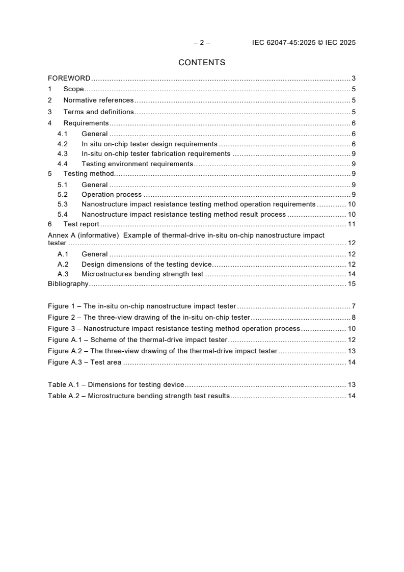
CONTENTS
FOREWORD . 3
1 Scope . 5
2 Normative references . 5
3 Terms and definitions . 5
4 Requirements . 6
4.1 General . 6
4.2 In situ on-chip tester design requirements . 6
4.3 In-situ on-chip tester fabrication requirements . 9
4.4 Testing environment requirements . 9
5 Testing method. 9
5.1 General . 9
5.2 Operation process . 9
5.3 Nanostructure impact resistance testing method operation requirements . 10
5.4 Nanostructure impact resistance testing method result process . 10
6 Test report . 11
Annex A (informative) Example of thermal-drive in-situ on-chip nanostructure impact
tester . 12
A.1 General . 12
A.2 Design dimensions of the testing device . 12
A.3 Microstructures bending strength test . 14
Bibliography . 15
Figure 1 – The in-situ on-chip nanostructure impact tester . 7
Figure 2 – The three-view drawing of the in-situ on-chip tester . 8
Figure 3 – Nanostructure impact resistance testing method operation process . 10
Figure A.1 – Scheme of the thermal-drive impact tester . 12
Figure A.2 – The three-view drawing of the thermal-drive impact tester . 13
Figure A.3 – Test area . 14
Table A.1 – Dimensions for testing device . 13
Table A.2 – Microstructure bending strength test results . 14
INTERNATIONAL ELECTROTECHNICAL COMMISSION
____________
SEMICONDUCTOR DEVICES –
MICRO-ELECTROMECHANICAL DEVICES –
Part 45: Silicon based MEMS fabrication technology –
Measurement method of impact resistance of nanostructures
FOREWORD
1) The International Electrotechnical Commission (IEC) is a worldwide organization for standardization comprising
all national electrotechnical committees (IEC National Committees). The object of IEC is to promote international
co-operation on all questions concerning standardization in the electrical and electronic fields. To this end and
in addition to other activities, IEC publishes International Standards, Technical Specifications, Technical Reports,
Publicly Available Specifications (PAS) and Guides (hereafter referred to as “IEC Publication(s)”). Their
preparation is entrusted to technical committees; any IEC National Committee interested in the subject dealt with
may participate in this preparatory work. International, governmental and non-governmental organizations liaising
with the IEC also participate in this preparation. IEC collaborates closely with the International Organization for
Standardization (ISO) in accordance with conditions determined by agreement between the two organizations.
2) The formal decisions or agreements of IEC on technical matters express, as nearly as possible, an international
consensus of opinion on the relevant subjects since each technical committee has representation from all
interested IEC National Committees.
3) IEC Publications have the form of recommendations for international use and are accepted by IEC National
Committees in that sense. While all reasonable efforts are made to ensure that the technical content of IEC
Publications is accurate, IEC cannot be held responsible for the way in which they are used or for any
misinterpretation by any end user.
4) In order to promote international uniformity, IEC National Committees undertake to apply IEC Publications
transparently to the maximum extent possible in their national and regional publications. Any divergence between
any IEC Publication and the corresponding national or regional publication shall be clearly indicated in the latter.
5) IEC itself does not provide any attestation of conformity. Independent certification bodies provide conformity
assessment services and, in some areas, access to IEC marks of conformity. IEC is not responsible for any
services carried out by independent certification bodies.
6) All users should ensure that they have the latest edition of this publication.
7) No liability shall attach to IEC or its directors, employees, servants or agents including individual experts and
members of its technical committees and IEC National Committees for any personal injury, property damage or
other damage of any nature whatsoever, whether direct or indirect, or for costs (including legal fees) and
expenses arising out of the publication, use of, or reliance upon, this IEC Publication or any other IEC
Publications.
8) Attention is drawn to the Normative references cited in this publication. Use of the referenced publications is
indispensable for the correct application of this publication.
9) IEC draws attention to the possibility that the implementation of this document may involve the use of (a)
patent(s). IEC takes no position concerning the evidence, validity or applicability of any claimed patent rights in
respect thereof. As of the date of publication of this document, IEC had not received notice of (a) patent(s), which
may be required to implement this document. However, implementers are cautioned that this may not represent
the latest information, which may be obtained from the patent database available at https://patents.iec.ch. IEC
shall not be held responsible for identifying any or all such patent rights.
IEC 62047-45 has been prepared by subcommittee 47F: Microelectromechanical systems, of
IEC technical committee 47: Semiconductor devices. It is an International Standard.
The text of this International Standard is based on the following documents:
Draft Report on voting
47F/497/FDIS 47F/504/RVD
Full information on the voting for its approval can be found in the report on voting indicated in
the above table.
The language used for the development of this International Standard is English.
– 4 – IEC 62047-45:2025 © IEC 2025
This document was drafted in accordance with ISO/IEC Directives, Part 2, and developed in
accordance with ISO/IEC Directives, Part 1 and ISO/IEC Directives, IEC Supplement, available
at www.iec.ch/members_experts/refdocs. The main document types developed by IEC are
described in greater detail at www.iec.ch/publications.
A list of all parts in the IEC 62047 series, published under the general title Semiconductor
devices – Micro-electromechanical devices, can be found on the IEC website.
The committee has decided that the contents of this document will remain unchanged until the
stability date indicated on the IEC website under webstore.iec.ch in the data related to the
specific document. At this date, the document will be
• reconfirmed,
• withdrawn, or
• revised.
SEMICONDUCTOR DEVICES –
MICRO-ELECTROMECHANICAL DEVICES –
Part 45: Silicon based MEMS fabrication technology –
Measurement method of impact resistance of nanostructures
1 Scope
This part of IEC 62047 specifies the requirements and testing method to measure the impact
resistance of nanostructures which are fabricated by micromachining technology used in silicon-
based micro-electromechanical system (MEMS).
This document is applicable to the in-situ impact resistance measurement of nanostructures
manufactured by microelectronic technology process and other micromachining technology.
In the production of MEMS devices, due to the micro/nano size, the non-ideal effect of
fabrication is greatly amplified compared with the macroscale. Surface defects, line width loss,
...


Questions, Comments and Discussion
Ask us and Technical Secretary will try to provide an answer. You can facilitate discussion about the standard in here.
Loading comments...