IEC 62047-47:2024
(Main)Semiconductor devices - Micro-electromechanical devices - Part 47: Silicon based MEMS fabrication technology - Measurement method of bending strength of microstructures
Semiconductor devices - Micro-electromechanical devices - Part 47: Silicon based MEMS fabrication technology - Measurement method of bending strength of microstructures
IEC 62047-47:2024 specifies the requirements and testing method to measure the bending strength of microstructures which are fabricated by micromachining technology used in silicon-based micro-electromechanical system (MEMS).
This document is applicable to the in-situ bending strength measurement of microstructures manufactured by microelectronic technology process and other micromachining technology.
With the devices scaling, the bending strength degradation, induced by defects and contaminations, becomes more severe. This document specifies an in-situ testing method of the bending strength based on MEMS technique. This document does not need intricate instruments (such as scanning probe microscopy and nanoindenter) and special test specimens.
Since in-situ on-chip tester in this document and device are fabricated with the same process on the same wafer, this document can give some practical reference for the design part.
General Information
- Status
- Published
- Publication Date
- 22-Aug-2024
- Technical Committee
- SC 47F - Micro-electromechanical systems
- Current Stage
- PPUB - Publication issued
- Start Date
- 23-Aug-2024
- Completion Date
- 20-Sep-2024
Overview
IEC 62047-47:2024 specifies an in‑situ measurement method for bending strength of microstructures fabricated by micromachining technology in silicon‑based MEMS. The standard defines requirements for an on‑chip tester (testing device + testing structure) that is fabricated with the same process and on the same wafer as the MEMS device, enabling on‑wafer, optical‑microscopy‑readable measurement of bending strength without requiring intricate instruments (for example scanning probe microscopy or nanoindenters).
Key topics and requirements
- Scope: Measurement of bending strength for microstructures manufactured by microelectronic and micromachining processes (silicon‑based MEMS).
- In‑situ on‑chip tester design:
- Use a beam of constant strength to reduce stress‑concentration and extraction errors.
- Include a testing device (displacement/deflection rulers, magnifying lever, elastic beam, on‑chip needlepoint, loading segment) to transfer and read force/displacement optically.
- Drive options: off‑chip probe loading (example), on‑chip thermal or electrostatic actuation.
- Ensure the elastic beam and bonding surfaces are stronger than the beam under test to force fracture in the test structure.
- Loading segment length requirement: l > 20 μm to limit linewidth loss influence to <5%.
- Ruler resolution must be compatible with optical microscopy.
- Account for machining tolerances and surface roughness from process steps.
- Fabrication:
- Tester and test structure must be fabricated using the same process as the MEMS device; applicable materials include movable structure layers such as crystalline silicon.
- Testing method:
- Fix the chip on a probe station, apply horizontal load until fracture while observing under optical microscope, record deflection ruler reading d, and compute bending strength per the document’s formula.
- Environment: Testing should be carried out in the device’s actual manufacturing environment (on‑wafer/wafer‑level).
Applications and who uses it
- Process and reliability engineers: wafer‑level mechanical property monitoring and process control.
- MEMS designers: design validation and guidance for durable microstructure layouts and bonding areas.
- Semiconductor fabs & test labs: on‑chip qualification and batch‑level screening for defects/contamination that degrade bending strength.
- R&D teams: comparative material and process evaluation without specialized nanoindentation equipment.
Benefits include practical, low‑cost wafer‑level testing, reduced reliance on specialized metrology, and direct relevance because the tester is co‑fabricated with devices.
Related standards
- Part of the IEC 62047 series (Semiconductor devices – Micro‑electromechanical devices).
- Definitions reference IEC 62047‑45:2024 where applicable.
Buy Documents
IEC 62047-47:2024 - Semiconductor devices - Micro-electromechanical devices - Part 47: Silicon based MEMS fabrication technology - Measurement method of bending strength of microstructures Released:8/23/2024 Isbn:9782832295564
Frequently Asked Questions
IEC 62047-47:2024 is a standard published by the International Electrotechnical Commission (IEC). Its full title is "Semiconductor devices - Micro-electromechanical devices - Part 47: Silicon based MEMS fabrication technology - Measurement method of bending strength of microstructures". This standard covers: IEC 62047-47:2024 specifies the requirements and testing method to measure the bending strength of microstructures which are fabricated by micromachining technology used in silicon-based micro-electromechanical system (MEMS). This document is applicable to the in-situ bending strength measurement of microstructures manufactured by microelectronic technology process and other micromachining technology. With the devices scaling, the bending strength degradation, induced by defects and contaminations, becomes more severe. This document specifies an in-situ testing method of the bending strength based on MEMS technique. This document does not need intricate instruments (such as scanning probe microscopy and nanoindenter) and special test specimens. Since in-situ on-chip tester in this document and device are fabricated with the same process on the same wafer, this document can give some practical reference for the design part.
IEC 62047-47:2024 specifies the requirements and testing method to measure the bending strength of microstructures which are fabricated by micromachining technology used in silicon-based micro-electromechanical system (MEMS). This document is applicable to the in-situ bending strength measurement of microstructures manufactured by microelectronic technology process and other micromachining technology. With the devices scaling, the bending strength degradation, induced by defects and contaminations, becomes more severe. This document specifies an in-situ testing method of the bending strength based on MEMS technique. This document does not need intricate instruments (such as scanning probe microscopy and nanoindenter) and special test specimens. Since in-situ on-chip tester in this document and device are fabricated with the same process on the same wafer, this document can give some practical reference for the design part.
IEC 62047-47:2024 is classified under the following ICS (International Classification for Standards) categories: 31.080.99 - Other semiconductor devices. The ICS classification helps identify the subject area and facilitates finding related standards.
IEC 62047-47:2024 is available in PDF format for immediate download after purchase. The document can be added to your cart and obtained through the secure checkout process. Digital delivery ensures instant access to the complete standard document.
Standards Content (Sample)
IEC 62047-47 ®
Edition 1.0 2024-08
INTERNATIONAL
STANDARD
Semiconductor devices – Micro-electromechanical devices –
Part 47: Silicon based MEMS fabrication technology – Measurement method of
bending strength of microstructures
All rights reserved. Unless otherwise specified, no part of this publication may be reproduced or utilized in any form
or by any means, electronic or mechanical, including photocopying and microfilm, without permission in writing from
either IEC or IEC's member National Committee in the country of the requester. If you have any questions about IEC
copyright or have an enquiry about obtaining additional rights to this publication, please contact the address below or
your local IEC member National Committee for further information.
IEC Secretariat Tel.: +41 22 919 02 11
3, rue de Varembé info@iec.ch
CH-1211 Geneva 20 www.iec.ch
Switzerland
About the IEC
The International Electrotechnical Commission (IEC) is the leading global organization that prepares and publishes
International Standards for all electrical, electronic and related technologies.
About IEC publications
The technical content of IEC publications is kept under constant review by the IEC. Please make sure that you have the
latest edition, a corrigendum or an amendment might have been published.
IEC publications search - webstore.iec.ch/advsearchform IEC Products & Services Portal - products.iec.ch
The advanced search enables to find IEC publications by a Discover our powerful search engine and read freely all the
variety of criteria (reference number, text, technical publications previews, graphical symbols and the glossary.
committee, …). It also gives information on projects, replaced With a subscription you will always have access to up to date
and withdrawn publications. content tailored to your needs.
IEC Just Published - webstore.iec.ch/justpublished
Electropedia - www.electropedia.org
Stay up to date on all new IEC publications. Just Published
The world's leading online dictionary on electrotechnology,
details all new publications released. Available online and once
containing more than 22 500 terminological entries in English
a month by email.
and French, with equivalent terms in 25 additional languages.
Also known as the International Electrotechnical Vocabulary
IEC Customer Service Centre - webstore.iec.ch/csc
(IEV) online.
If you wish to give us your feedback on this publication or need
further assistance, please contact the Customer Service
Centre: sales@iec.ch.
IEC 62047-47 ®
Edition 1.0 2024-08
INTERNATIONAL
STANDARD
Semiconductor devices – Micro-electromechanical devices –
Part 47: Silicon based MEMS fabrication technology – Measurement method of
bending strength of microstructures
INTERNATIONAL
ELECTROTECHNICAL
COMMISSION
ICS 31.080.99 ISBN 978-2-8322-9556-4
– 2 – IEC 62047-47:2024 © IEC 2024
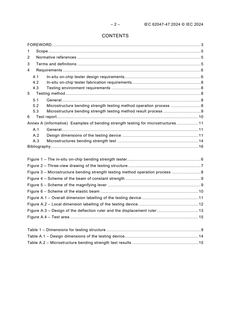
CONTENTS
FOREWORD . 3
1 Scope . 5
2 Normative references . 5
3 Terms and definitions . 5
4 Requirements . 6
4.1 In-situ on-chip tester design requirements . 6
4.2 In-situ on-chip tester fabrication requirements . 8
4.3 Testing environment requirements . 8
5 Testing method . 8
5.1 General . 8
5.2 Microstructure bending strength testing method operation process . 8
5.3 Microstructure bending strength testing method result process . 9
6 Test report . 10
Annex A (informative) Examples of bending strength testing for microstructures . 11
A.1 General . 11
A.2 Design dimensions of the testing device . 11
A.3 Microstructures bending strength test . 14
Bibliography . 16
Figure 1 – The in-situ on-chip bending strength tester. 6
Figure 2 – Three-view drawing of the testing structure . 7
Figure 3 – Microstructure bending strength testing method operation process . 8
Figure 4 – Scheme of the beam of constant strength . 9
Figure 5 – Scheme of the magnifying lever . 9
Figure 6 – Scheme of the elastic beam . 10
Figure A.1 – Overall dimension labelling of the testing device . 11
Figure A.2 – Local dimension labelling of the testing device . 12
Figure A.3 – Design of the deflection ruler and the displacement ruler . 13
Figure A.4 – Test area . 15
Table 1 – Dimensions for testing structure . 9
Table A.1 – Design dimensions of the testing device. 14
Table A.2 – Microstructure bending strength test results . 15
INTERNATIONAL ELECTROTECHNICAL COMMISSION
____________
SEMICONDUCTOR DEVICES –
MICRO-ELECTROMECHANICAL DEVICES –
Part 47: Silicon based MEMS fabrication technology –
Measurement method of bending strength of microstructures
FOREWORD
1) The International Electrotechnical Commission (IEC) is a worldwide organization for standardization comprising
all national electrotechnical committees (IEC National Committees). The object of IEC is to promote international
co-operation on all questions concerning standardization in the electrical and electronic fields. To this end and
in addition to other activities, IEC publishes International Standards, Technical Specifications, Technical Reports,
Publicly Available Specifications (PAS) and Guides (hereafter referred to as "IEC Publication(s)"). Their
preparation is entrusted to technical committees; any IEC National Committee interested in the subject dealt with
may participate in this preparatory work. International, governmental and non-governmental organizations liaising
with the IEC also participate in this preparation. IEC collaborates closely with the International Organization for
Standardization (ISO) in accordance with conditions determined by agreement between the two organizations.
2) The formal decisions or agreements of IEC on technical matters express, as nearly as possible, an international
consensus of opinion on the relevant subjects since each technical committee has representation from all
interested IEC National Committees.
3) IEC Publications have the form of recommendations for international use and are accepted by IEC National
Committees in that sense. While all reasonable efforts are made to ensure that the technical content of IEC
Publications is accurate, IEC cannot be held responsible for the way in which they are used or for any
misinterpretation by any end user.
4) In order to promote international uniformity, IEC National Committees undertake to apply IEC Publications
transparently to the maximum extent possible in their national and regional publications. Any divergence between
any IEC Publication and the corresponding national or regional publication shall be clearly indicated in the latter.
5) IEC itself does not provide any attestation of conformity. Independent certification bodies provide conformity
assessment services and, in some areas, access to IEC marks of conformity. IEC is not responsible for any
services carried out by independent certification bodies.
6) All users should ensure that they have the latest edition of this publication.
7) No liability shall attach to IEC or its directors, employees, servants or agents including individual experts and
members of its technical committees and IEC National Committees for any personal injury, property damage or
other damage of any nature whatsoever, whether direct or indirect, or for costs (including legal fees) and
expenses arising out of the publication, use of, or reliance upon, this IEC Publication or any other IEC
Publications.
8) Attention is drawn to the Normative references cited in this publication. Use of the referenced publications is
indispensable for the correct application of this publication.
9) IEC draws attention to the possibility that the implementation of this document may involve the use of (a)
patent(s). IEC takes no position concerning the evidence, validity or applicability of any claimed patent rights in
respect thereof. As of the date of publication of this document, IEC had not received notice of (a) patent(s), which
may be required to implement this document. However, implementers are cautioned that this may not represent
the latest information, which may be obtained from the patent database available at https://patents.iec.ch. IEC
shall not be held responsible for identifying any or all such patent rights.
IEC 62047-47 has been prepared by subcommittee 47F: Micro-electromechanical systems, of
IEC technical committee 47: Semiconductor devices. It is an International Standard.
The text of this International Standard is based on the following documents:
Draft Report on voting
47F/474/FDIS 47F/481/RVD
Full information on the voting for its approval can be found in the report on voting indicated in
the above table.
– 4 – IEC 62047-47:2024 © IEC 2024
The language used for the development of this International Standard is English.
This document was drafted in accordance with ISO/IEC Directives, Part 2, and developed in
accordance with ISO/IEC Directives, Part 1 and ISO/IEC Directives, IEC Supplement, available
at www.iec.ch/members_experts/refdocs. The main document types developed by IEC are
described in greater detail at www.iec.ch/publications.
A list of all parts in the IEC 62047 series, published under the general title Semiconductor
devices – Micro-electromechanical devices, can be found on the IEC website.
The committee has decided that the contents of this document will remain unchanged until the
stability date indicated on the IEC website under webstore.iec.ch in the data related to the
specific document. At this date, the document will be
• reconfirmed,
• withdrawn, or
• revised.
IMPORTANT – The "colour inside" logo on the cover page of this document indicates
that it contains colours which are considered to be useful for the correct understanding
of its contents. Users should therefore print this document using a colour printer.
SEMICONDUCTOR DEVICES –
MICRO-ELECTROMECHANICAL DEVICES –
Part 47: Silicon based MEMS fabrication technology –
Measurement method of bending strength of microstructures
1 Scope
This part of IEC 62047 specifies the requirements and testing method to measure the bending
stre
...


Questions, Comments and Discussion
Ask us and Technical Secretary will try to provide an answer. You can facilitate discussion about the standard in here.
Loading comments...