IEC 62047-31:2019
(Main)Semiconductor devices - Micro-electromechanical devices - Part 31: Four-point bending test method for interfacial adhesion energy of layered MEMS materials
Semiconductor devices - Micro-electromechanical devices - Part 31: Four-point bending test method for interfacial adhesion energy of layered MEMS materials
IEC 62047-31:2019 (E) specifies a four-point bending test method for measuring interfacial adhesion energy of the weakest interface in the layered micro-electromechanical systems (MEMS) based on the concept of fracture mechanics. In a variety of MEMS devices, there are many layered material interfaces, and their adhesion energies are critical to the reliability of the MEMS devices. The four-point bending test utilizes a pure bending moment applied to a test piece of layered MEMS device, and the interfacial adhesion energy is measured from the critical bending moment for the steady state cracking in the weakest interface. This test method applies to MEMS devices with thin film layers deposited on semiconductor substrates. The total thickness of the thin film layers should be 100 times less than the thickness of a supporting substrate (typically a silicon wafer piece).
General Information
- Status
- Published
- Publication Date
- 04-Apr-2019
- Technical Committee
- SC 47F - Micro-electromechanical systems
- Current Stage
- PPUB - Publication issued
- Start Date
- 05-Apr-2019
- Completion Date
- 26-Apr-2019
Overview
IEC 62047-31:2019 specifies a standardized four-point bending test method to measure the interfacial adhesion energy (critical energy release rate) of the weakest interface in layered MEMS materials. Based on fracture mechanics, the method applies to thin-film stacks deposited on semiconductor substrates (typically silicon) where the total thin-film thickness is much smaller than the supporting substrate. The test uses a pure bending moment applied to a machined test piece to initiate and propagate steady-state interfacial cracking; the interfacial adhesion energy is derived from the critical bending load.
Key topics and requirements
- Test principle: Introduce a pre-crack/notch, initiate a crack that reaches the weakest interface, then reload to measure the critical load for steady-state interfacial crack growth. Under pure bending the energy release rate is independent of crack length.
- Test piece geometry and fabrication:
- Test pieces must be produced using the same fabrication process as the actual MEMS devices.
- Geometry constraints: thickness of the test piece should be ~50× less than its length and width; length should be ~10× larger than width. Total thin-film thickness should be ~100× less than the supporting substrate thickness.
- Pre-crack/notch may be made by diamond saw, laser ablation or chemical etching.
- Measurements and tolerances:
- Dimensional measurements for span (L), width (b) and substrate thickness (h) must be accurate (error < ±5%).
- The standard provides the fracture‑mechanics equation to compute energy release rate from the applied load (P), span (L), Young’s modulus (E), Poisson’s ratio (ν), width (b) and substrate thickness (h).
- Test apparatus and control:
- Four-point bending fixture on a universal testing machine with load cell, actuator, linear guide and displacement sensor.
- Loading pin diameter requirements (as specified in the standard), and instrumentation resolution requirements (load cell and displacement sensor resolutions < 1/100 of relevant values).
- Loading speed range recommended for steady-state cracking and camera imaging at >10 Hz with ≥20× magnification for crack behavior recording.
Applications
- Thin-film adhesion characterization for MEMS components (sensors, actuators, RF-MEMS, micro-optics).
- Process qualification and materials selection during MEMS fabrication development.
- Failure analysis and reliability assessment where interfacial delamination is a root cause.
- Comparative testing of surface treatments, adhesion layers and deposition processes.
Who should use this standard
- MEMS designers and process engineers
- Reliability and failure‑analysis laboratories
- Materials scientists working on thin-film adhesion
- Semiconductor test labs and QA teams validating MEMS fabrication
Related standards
- Other parts of the IEC 62047 series (Semiconductor devices – Micro‑electromechanical devices)
- IEC 62047-2 and IEC 62047-3 are referenced for thickness measurement methods used in preparing and analyzing test pieces.
Keywords: IEC 62047-31, four-point bending, interfacial adhesion energy, layered MEMS materials, thin film adhesion, fracture mechanics test, MEMS reliability.
Frequently Asked Questions
IEC 62047-31:2019 is a standard published by the International Electrotechnical Commission (IEC). Its full title is "Semiconductor devices - Micro-electromechanical devices - Part 31: Four-point bending test method for interfacial adhesion energy of layered MEMS materials". This standard covers: IEC 62047-31:2019 (E) specifies a four-point bending test method for measuring interfacial adhesion energy of the weakest interface in the layered micro-electromechanical systems (MEMS) based on the concept of fracture mechanics. In a variety of MEMS devices, there are many layered material interfaces, and their adhesion energies are critical to the reliability of the MEMS devices. The four-point bending test utilizes a pure bending moment applied to a test piece of layered MEMS device, and the interfacial adhesion energy is measured from the critical bending moment for the steady state cracking in the weakest interface. This test method applies to MEMS devices with thin film layers deposited on semiconductor substrates. The total thickness of the thin film layers should be 100 times less than the thickness of a supporting substrate (typically a silicon wafer piece).
IEC 62047-31:2019 (E) specifies a four-point bending test method for measuring interfacial adhesion energy of the weakest interface in the layered micro-electromechanical systems (MEMS) based on the concept of fracture mechanics. In a variety of MEMS devices, there are many layered material interfaces, and their adhesion energies are critical to the reliability of the MEMS devices. The four-point bending test utilizes a pure bending moment applied to a test piece of layered MEMS device, and the interfacial adhesion energy is measured from the critical bending moment for the steady state cracking in the weakest interface. This test method applies to MEMS devices with thin film layers deposited on semiconductor substrates. The total thickness of the thin film layers should be 100 times less than the thickness of a supporting substrate (typically a silicon wafer piece).
IEC 62047-31:2019 is classified under the following ICS (International Classification for Standards) categories: 31.080.99 - Other semiconductor devices. The ICS classification helps identify the subject area and facilitates finding related standards.
IEC 62047-31:2019 is available in PDF format for immediate download after purchase. The document can be added to your cart and obtained through the secure checkout process. Digital delivery ensures instant access to the complete standard document.
Standards Content (Sample)
IEC 62047-31 ®
Edition 1.0 2019-04
INTERNATIONAL
STANDARD
colour
inside
Semiconductor devices – Micro-electromechanical devices –
Part 31: Four-point bending test method for interfacial adhesion energy of
layered MEMS materials
All rights reserved. Unless otherwise specified, no part of this publication may be reproduced or utilized in any form
or by any means, electronic or mechanical, including photocopying and microfilm, without permission in writing from
either IEC or IEC's member National Committee in the country of the requester. If you have any questions about IEC
copyright or have an enquiry about obtaining additional rights to this publication, please contact the address below or
your local IEC member National Committee for further information.
IEC Central Office Tel.: +41 22 919 02 11
3, rue de Varembé info@iec.ch
CH-1211 Geneva 20 www.iec.ch
Switzerland
About the IEC
The International Electrotechnical Commission (IEC) is the leading global organization that prepares and publishes
International Standards for all electrical, electronic and related technologies.
About IEC publications
The technical content of IEC publications is kept under constant review by the IEC. Please make sure that you have the
latest edition, a corrigendum or an amendment might have been published.
IEC publications search - webstore.iec.ch/advsearchform Electropedia - www.electropedia.org
The advanced search enables to find IEC publications by a The world's leading online dictionary on electrotechnology,
variety of criteria (reference number, text, technical containing more than 22 000 terminological entries in English
committee,…). It also gives information on projects, replaced and French, with equivalent terms in 16 additional languages.
and withdrawn publications. Also known as the International Electrotechnical Vocabulary
(IEV) online.
IEC Just Published - webstore.iec.ch/justpublished
Stay up to date on all new IEC publications. Just Published IEC Glossary - std.iec.ch/glossary
details all new publications released. Available online and 67 000 electrotechnical terminology entries in English and
once a month by email. French extracted from the Terms and Definitions clause of
IEC publications issued since 2002. Some entries have been
IEC Customer Service Centre - webstore.iec.ch/csc collected from earlier publications of IEC TC 37, 77, 86 and
If you wish to give us your feedback on this publication or CISPR.
need further assistance, please contact the Customer Service
Centre: sales@iec.ch.
IEC 62047-31 ®
Edition 1.0 2019-04
INTERNATIONAL
STANDARD
colour
inside
Semiconductor devices – Micro-electromechanical devices –
Part 31: Four-point bending test method for interfacial adhesion energy of
layered MEMS materials
INTERNATIONAL
ELECTROTECHNICAL
COMMISSION
ICS 31.080.99 ISBN 978-2-8322-6717-2
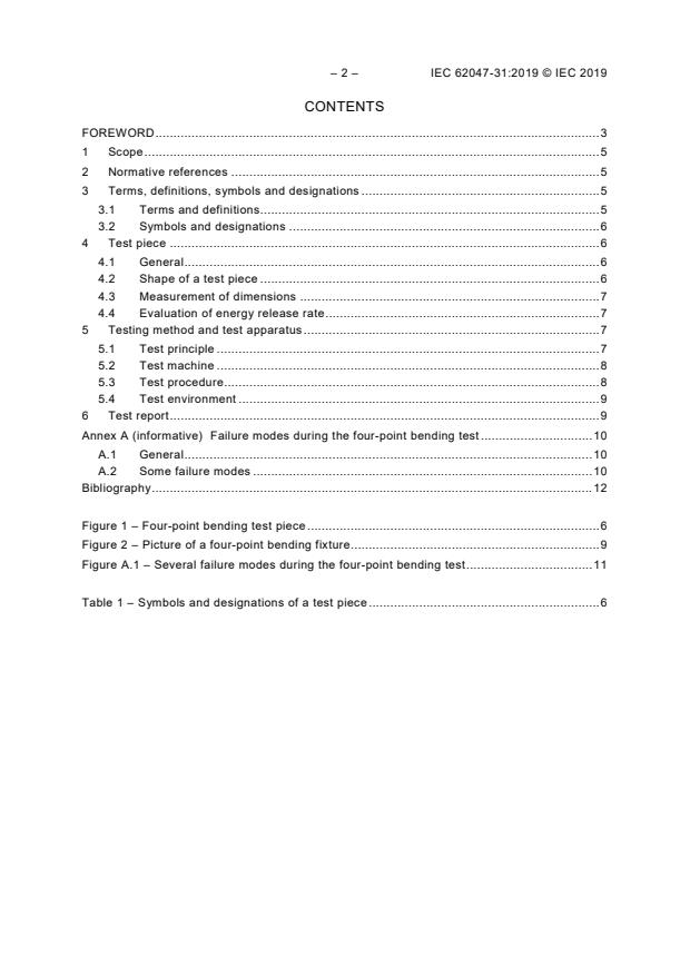
– 2 – IEC 62047-31:2019 © IEC 2019
CONTENTS
FOREWORD . 3
1 Scope . 5
2 Normative references . 5
3 Terms, definitions, symbols and designations . 5
3.1 Terms and definitions . 5
3.2 Symbols and designations . 6
4 Test piece . 6
4.1 General . 6
4.2 Shape of a test piece . 6
4.3 Measurement of dimensions . 7
4.4 Evaluation of energy release rate . 7
5 Testing method and test apparatus . 7
5.1 Test principle . 7
5.2 Test machine . 8
5.3 Test procedure . 8
5.4 Test environment . 9
6 Test report . 9
Annex A (informative) Failure modes during the four-point bending test . 10
A.1 General . 10
A.2 Some failure modes . 10
Bibliography . 12
Figure 1 – Four-point bending test piece . 6
Figure 2 – Picture of a four-point bending fixture . 9
Figure A.1 – Several failure modes during the four-point bending test . 11
Table 1 – Symbols and designations of a test piece . 6
INTERNATIONAL ELECTROTECHNICAL COMMISSION
____________
SEMICONDUCTOR DEVICES –
MICRO-ELECTROMECHANICAL DEVICES –
Part 31: Four-point bending test method for interfacial
adhesion energy of layered MEMS materials
FOREWORD
1) The International Electrotechnical Commission (IEC) is a worldwide organization for standardization comprising
all national electrotechnical committees (IEC National Committees). The object of IEC is to promote
international co-operation on all questions concerning standardization in the electrical and electronic fields. To
this end and in addition to other activities, IEC publishes International Standards, Technical Specifications,
Technical Reports, Publicly Available Specifications (PAS) and Guides (hereafter referred to as “IEC
Publication(s)”). Their preparation is entrusted to technical committees; any IEC National Committee interested
in the subject dealt with may participate in this preparatory work. International, governmental and non-
governmental organizations liaising with the IEC also participate in this preparation. IEC collaborates closely
with the International Organization for Standardization (ISO) in accordance with conditions determined by
agreement between the two organizations.
2) The formal decisions or agreements of IEC on technical matters express, as nearly as possible, an international
consensus of opinion on the relevant subjects since each technical committee has representation from all
interested IEC National Committees.
3) IEC Publications have the form of recommendations for international use and are accepted by IEC National
Committees in that sense. While all reasonable efforts are made to ensure that the technical content of IEC
Publications is accurate, IEC cannot be held responsible for the way in which they are used or for any
misinterpretation by any end user.
4) In order to promote international uniformity, IEC National Committees undertake to apply IEC Publications
transparently to the maximum extent possible in their national and regional publications. Any divergence
between any IEC Publication and the corresponding national or regional publication shall be clearly indicated in
the latter.
5) IEC itself does not provide any attestation of conformity. Independent certification bodies provide conformity
assessment services and, in some areas, access to IEC marks of conformity. IEC is not responsible for any
services carried out by independent certification bodies.
6) All users should ensure that they have the latest edition of this publication.
7) No liability shall attach to IEC or its directors, employees, servants or agents including individual experts and
members of its technical committees and IEC National Committees for any personal injury, property damage or
other damage of any nature whatsoever, whether direct or indirect, or for costs (including legal fees) and
expenses arising out of the publication, use of, or reliance upon, this IEC Publication or any other IEC
Publications.
8) Attention is drawn to the Normative references cited in this publication. Use of the referenced publications is
indispensable for the correct application of this publication.
9) Attention is drawn to the possibility that some of the elements of this IEC Publication may be the subject of
patent rights. IEC shall not be held responsible for identifying any or all such patent rights.
International Standard IEC 62047-31 has been prepared by subcommittee 47F: Micro-
electromechanical systems, of IEC technical committee 47: Semiconductor devices.
The text of this International Standard is based on the following documents:
FDIS Report on voting
47F/326/FDIS 47F/331RVD
Full information on the voting for the approval of this International Standard can be found in
the report on voting indicated in the above table.
This document has been drafted in accordance with the ISO/IEC Directives, Part 2.
– 4 – IEC 62047-31:2019 © IEC 2019
A list of all parts in the IEC 62047 series, published under the general title Semiconductor
devices – Micro-electromechanical devices, can be found on the IEC website.
The committee has decided that the contents of this document will remain unchanged until the
stability date indicated on the IEC website under "http://webstore.iec.ch" in the data related to
the specific document. At this date, the document will be
• reconfirmed,
• withdrawn,
• replaced by a revised edition, or
• amended.
A bilingual version of this publication may be issued at a later date.
IMPORTANT – The 'colour inside' logo on the cover page of this publication indicates
that it contains colours which are considered to be useful for the correct
understanding of its contents. Users should therefore print this document using a
colour printer.
SEMICONDUCTOR DEVICES –
MICRO-ELECTROMECHANICAL DEVICES –
Part 31: Four-point bending test method for interfacial
adhesion energy of layered MEMS materials
1 Scope
This part of IEC 62047 specifies a four-point bending test method for measuring interfacial
adhesion energy of the weakest interface in the layered micro-electromechanical systems
(MEMS) based on the concept of fracture mechanics. In a variety of MEMS devices, there are
many layered material interfaces, and their adhesion energies are critical to the reliability of
the MEMS devices. The four-point bending test utilizes a pure bending moment applied to a
test piece of layered MEMS device, and the interfacial adhesion energy is measured from the
critical bending moment for the steady state cracking in the weakest interface. This test
method applies to MEMS devices with thin film layers deposited on semiconductor substrates.
The total thickness of the thin film layers should be 100 times less than the thickness of a
supporting substrate (typically a silicon wafer piece).
2 Normative references
The following documents are referred to in the text in such a way that some or all of their
content constitutes requirements of this document. For dated references, only the edition
cited applies. For undated references, the latest edition of the referenced document (including
any amendments) applies.
There are no normative references in this document.
3 Te
...


Questions, Comments and Discussion
Ask us and Technical Secretary will try to provide an answer. You can facilitate discussion about the standard in here.
Loading comments...