IEC TS 61994-4-4:2018
(Main)Piezoelectric, dielectric and electrostatic devices and associated materials for frequency control, selection and detection - Glossary - Part 4-4: Piezoelectric materials - Single crystal wafers for surface acoustic wave (SAW) devices
Piezoelectric, dielectric and electrostatic devices and associated materials for frequency control, selection and detection - Glossary - Part 4-4: Piezoelectric materials - Single crystal wafers for surface acoustic wave (SAW) devices
IEC 61994-4-4:2018 gives the terms and definition for single crystal wafers for surface acoustic wave (SAW) devices representing the state of the art. This edition includes the following significant technical changes with respect to the previous edition:
- the new terms and definitions given in IEC 62276:2016 have been taken into account;
- the general title has been changed according to the change in the title of TC 49 in 2009.
- the part title has been changed according to the title of IEC 62276:2016.
General Information
- Status
- Published
- Publication Date
- 15-Nov-2018
- Technical Committee
- TC 49 - Piezoelectric, dielectric and electrostatic devices and associated materials for frequency control, selection and detection
- Drafting Committee
- WG 11 - TC 49/WG 11
- Current Stage
- PPUB - Publication issued
- Start Date
- 16-Nov-2018
- Completion Date
- 26-Oct-2018
Relations
- Effective Date
- 05-Sep-2023
Overview
IEC TS 61994-4-4:2018 is a technical specification published by the International Electrotechnical Commission (IEC) that defines a comprehensive glossary for single crystal wafers used in surface acoustic wave (SAW) devices. Part of the broader IEC 61994 series, this document targets piezoelectric, dielectric, and electrostatic materials and devices crucial for frequency control, selection, and detection applications. This edition incorporates updated terminology in alignment with IEC 62276:2016 and reflects changes in related technical committee titles, signifying its adherence to the current state of the art.
The use of standardized definitions supports clear communication and precise specification throughout the electronics industry, especially vital in sectors focusing on advanced frequency control and filtering components.
Key Topics
IEC TS 61994-4-4:2018 covers terminology and definitions relevant to:
- Single Crystal Wafer Materials for SAW Devices
- As-grown synthetic quartz crystal
- Lithium niobate (LN)
- Lithium tantalate (LT)
- Lanthanum gallium silicate (LGS)
- Lithium tetraborate (LBO)
- SAW Device Wafer Properties
- Flatness metrics, including site-specific and total thickness variation
- Crystal orientation and methods of specification
- Appearance defects (chips, scratches, pits, orange peel)
- Process-Specific Terms
- Curie temperature
- Polarization and reduction processes
- Single domain characteristics
- Manufacturing and Quality Aspects
- Bevel, orientation flat (OF), secondary flat (SF)
- Manufacturing lots and tolerance definitions
The document integrates updated terminology to facilitate a consistent language for materials selection, processing, metrology, and device manufacturing.
Applications
The standardized glossary provided in IEC TS 61994-4-4:2018 is applicable across multiple stages and sectors involved in SAW device development and use:
- Component Manufacturing:
Clear terms for piezoelectric single crystal wafers help manufacturers specify, verify, and communicate material requirements and quality metrics with suppliers and clients. - Research and Development:
Researchers benefit from uniform definitions when pioneering new SAW materials, optimizing wafer properties, or designing innovative frequency control devices. - Quality Assurance and Metrology:
Consistent descriptors of defects, surface conditions, and geometric tolerances underpin standardized inspection and measurement methods, ensuring product conformance. - Procurement and Supply Chain:
Accurate terminology reduces the risk of misinterpretation in technical specifications, tender documents, and supply agreements.
These applications are particularly relevant to sectors such as telecommunications, signal processing, sensors, and precision timing, where SAW technology plays a critical role.
Related Standards
For comprehensive implementation, IEC TS 61994-4-4:2018 should be considered in conjunction with related standards, including:
- IEC 62276:2016
Single Crystal Wafers for Surface Acoustic Wave (SAW) Device Applications – Specifications and Measuring Methods
Provides detailed specifications and measurement methodologies for the properties and performance of SAW device wafers. - Other parts of IEC 61994 series
Offer additional terminology and guidelines for piezoelectric, dielectric, and electrostatic materials and components. - IEC Electropedia
An online resource for cross-referencing electrotechnical vocabulary as used in international standards.
By leveraging IEC TS 61994-4-4:2018, stakeholders benefit from a harmonized vocabulary that streamlines cross-industry collaboration, improves product quality, and supports ongoing technical innovation in the field of SAW device materials.
Buy Documents
IEC TS 61994-4-4:2018 - Piezoelectric, dielectric and electrostatic devices and associated materials for frequency control, selection and detection - Glossary - Part 4-4: Piezoelectric materials - Single crystal wafers for surface acoustic wave (SAW) devices Released:11/16/2018
IEC TS 61994-4-4:2018 RLV - Piezoelectric, dielectric and electrostatic devices and associated materials for frequency control, selection and detection - Glossary - Part 4-4: Piezoelectric materials - Single crystal wafers for surface acoustic wave (SAW) devices Released:11/16/2018
Frequently Asked Questions
IEC TS 61994-4-4:2018 is a technical specification published by the International Electrotechnical Commission (IEC). Its full title is "Piezoelectric, dielectric and electrostatic devices and associated materials for frequency control, selection and detection - Glossary - Part 4-4: Piezoelectric materials - Single crystal wafers for surface acoustic wave (SAW) devices". This standard covers: IEC 61994-4-4:2018 gives the terms and definition for single crystal wafers for surface acoustic wave (SAW) devices representing the state of the art. This edition includes the following significant technical changes with respect to the previous edition: - the new terms and definitions given in IEC 62276:2016 have been taken into account; - the general title has been changed according to the change in the title of TC 49 in 2009. - the part title has been changed according to the title of IEC 62276:2016.
IEC 61994-4-4:2018 gives the terms and definition for single crystal wafers for surface acoustic wave (SAW) devices representing the state of the art. This edition includes the following significant technical changes with respect to the previous edition: - the new terms and definitions given in IEC 62276:2016 have been taken into account; - the general title has been changed according to the change in the title of TC 49 in 2009. - the part title has been changed according to the title of IEC 62276:2016.
IEC TS 61994-4-4:2018 is classified under the following ICS (International Classification for Standards) categories: 01.040.31 - Electronics (Vocabularies); 31.140 - Piezoelectric devices. The ICS classification helps identify the subject area and facilitates finding related standards.
IEC TS 61994-4-4:2018 has the following relationships with other standards: It is inter standard links to IEC TS 61994-4-4:2010. Understanding these relationships helps ensure you are using the most current and applicable version of the standard.
IEC TS 61994-4-4:2018 is available in PDF format for immediate download after purchase. The document can be added to your cart and obtained through the secure checkout process. Digital delivery ensures instant access to the complete standard document.
Standards Content (Sample)
IEC TS 61994-4-4 ®
Edition 3.0 2018-11
TECHNICAL
SPECIFICATION
Piezoelectric, dielectric and electrostatic devices and associated materials for
frequency control, selection and detection – Glossary –
Part 4-4: Piezoelectric materials – Single crystal wafers for surface acoustic
wave (SAW) devices
All rights reserved. Unless otherwise specified, no part of this publication may be reproduced or utilized in any form
or by any means, electronic or mechanical, including photocopying and microfilm, without permission in writing from
either IEC or IEC's member National Committee in the country of the requester. If you have any questions about IEC
copyright or have an enquiry about obtaining additional rights to this publication, please contact the address below or
your local IEC member National Committee for further information.
IEC Central Office Tel.: +41 22 919 02 11
3, rue de Varembé info@iec.ch
CH-1211 Geneva 20 www.iec.ch
Switzerland
About the IEC
The International Electrotechnical Commission (IEC) is the leading global organization that prepares and publishes
International Standards for all electrical, electronic and related technologies.
About IEC publications
The technical content of IEC publications is kept under constant review by the IEC. Please make sure that you have the
latest edition, a corrigenda or an amendment might have been published.
IEC Catalogue - webstore.iec.ch/catalogue Electropedia - www.electropedia.org
The stand-alone application for consulting the entire The world's leading online dictionary of electronic and
bibliographical information on IEC International Standards, electrical terms containing 21 000 terms and definitions in
Technical Specifications, Technical Reports and other English and French, with equivalent terms in 16 additional
documents. Available for PC, Mac OS, Android Tablets and languages. Also known as the International Electrotechnical
iPad. Vocabulary (IEV) online.
IEC publications search - webstore.iec.ch/advsearchform IEC Glossary - std.iec.ch/glossary
The advanced search enables to find IEC publications by a 67 000 electrotechnical terminology entries in English and
variety of criteria (reference number, text, technical French extracted from the Terms and Definitions clause of
committee,…). It also gives information on projects, replaced IEC publications issued since 2002. Some entries have been
and withdrawn publications. collected from earlier publications of IEC TC 37, 77, 86 and
CISPR.
IEC Just Published - webstore.iec.ch/justpublished
Stay up to date on all new IEC publications. Just Published IEC Customer Service Centre - webstore.iec.ch/csc
details all new publications released. Available online and If you wish to give us your feedback on this publication or
also once a month by email. need further assistance, please contact the Customer Service
Centre: sales@iec.ch.
IEC TS 61994-4-4 ®
Edition 3.0 2018-11
TECHNICAL
SPECIFICATION
Piezoelectric, dielectric and electrostatic devices and associated materials for
frequency control, selection and detection – Glossary –
Part 4-4: Piezoelectric materials – Single crystal wafers for surface acoustic
wave (SAW) devices
INTERNATIONAL
ELECTROTECHNICAL
COMMISSION
ICS 01.040.31; 31.140 ISBN 978-2-8322-6178-1
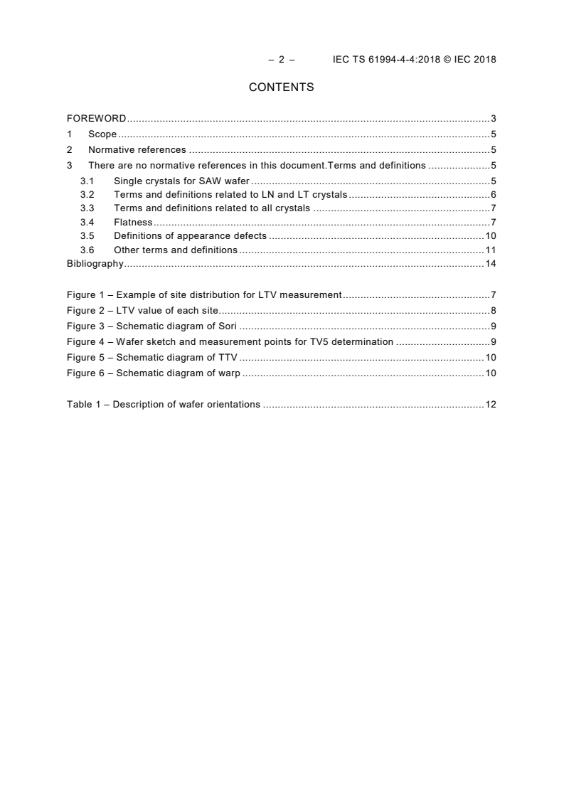
– 2 – IEC TS 61994-4-4:2018 © IEC 2018
CONTENTS
FOREWORD . 3
1 Scope . 5
2 Normative references . 5
3 There are no normative references in this document.Terms and definitions . 5
3.1 Single crystals for SAW wafer . 5
3.2 Terms and definitions related to LN and LT crystals . 6
3.3 Terms and definitions related to all crystals . 7
3.4 Flatness . 7
3.5 Definitions of appearance defects . 10
3.6 Other terms and definitions . 11
Bibliography . 14
Figure 1 – Example of site distribution for LTV measurement . 7
Figure 2 – LTV value of each site . 8
Figure 3 – Schematic diagram of Sori . 9
Figure 4 – Wafer sketch and measurement points for TV5 determination . 9
Figure 5 – Schematic diagram of TTV . 10
Figure 6 – Schematic diagram of warp . 10
Table 1 – Description of wafer orientations . 12
INTERNATIONAL ELECTROTECHNICAL COMMISSION
____________
PIEZOELECTRIC, DIELECTRIC AND ELECTROSTATIC DEVICES
AND ASSOCIATED MATERIALS FOR FREQUENCY CONTROL, SELECTION
AND DETECTION – GLOSSARY –
Part 4-4: Piezoelectric materials – Single crystal wafers
for surface acoustic wave (SAW) devices
FOREWORD
1) The International Electrotechnical Commission (IEC) is a worldwide organization for standardization comprising
all national electrotechnical committees (IEC National Committees). The object of IEC is to promote international
co-operation on all questions concerning standardization in the electrical and electronic fields. To this end and in
addition to other activities, IEC publishes International Standards, Technical Specifications, Technical Reports,
Publicly Available Specifications (PAS) and Guides (hereafter referred to as “IEC Publication(s)”). Their
preparation is entrusted to technical committees; any IEC National Committee interested in the subject dealt with
may participate in this preparatory work. International, governmental and non-governmental organizations liaising
with the IEC also participate in this preparation. IEC collaborates closely with the International Organization for
Standardization (ISO) in accordance with conditions determined by agreement between the two organizations.
2) The formal decisions or agreements of IEC on technical matters express, as nearly as possible, an international
consensus of opinion on the relevant subjects since each technical committee has representation from all
interested IEC National Committees.
3) IEC Publications have the form of recommendations for international use and are accepted by IEC National
Committees in that sense. While all reasonable efforts are made to ensure that the technical content of IEC
Publications is accurate, IEC cannot be held responsible for the way in which they are used or for any
misinterpretation by any end user.
4) In order to promote international uniformity, IEC National Committees undertake to apply IEC Publications
transparently to the maximum extent possible in their national and regional publications. Any divergence between
any IEC Publication and the corresponding national or regional publication shall be clearly indicated in the latter.
5) IEC itself does not provide any attestation of conformity. Independent certification bodies provide conformity
assessment services and, in some areas, access to IEC marks of conformity. IEC is not responsible for any
services carried out by independent certification bodies.
6) All users should ensure that they have the latest edition of this publication.
7) No liability shall attach to IEC or its directors, employees, servants or agents including individual experts and
members of its technical committees and IEC National Committees for any personal injury, property damage or
other damage of any nature whatsoever, whether direct or indirect, or for costs (including legal fees) and expenses
arising out of the publication, use of, or reliance upon, this IEC Publication or any other IEC Publications.
8) Attention is drawn to the Normative references cited in this publication. Use of the referenced publications is
indispensable for the correct application of this publication.
9) Attention is drawn to the possibility that some of the elements of this IEC Publication may be the subject of patent
rights. IEC shall not be held responsible for identifying any or all such patent rights.
The main task of IEC technical committees is to prepare International Standards. In exceptional
circumstances, a technical committee may propose the publication of a technical specification
when
• the required support cannot be obtained for the publication of an International Standard,
despite repeated efforts, or
• the subject is still under technical development or where, for any other reason, there is the
future but no immediate possibility of an agreement on an International Standard.
Technical specifications are subject to review within three years of publication to decide whether
they can be transformed into International Standards.
IEC TS 61944-4-4, which is a technical specification, has been prepared by IEC technical
committee 49: Piezoelectric, dielectric and electrostatic devices and associated materials for
frequency control, selection and detection.
– 4 – IEC TS 61994-4-4:2018 © IEC 2018
This third edition of IEC 61994-4-4 cancels and replaces the second edition published in 2010.
This edition constitutes a technical revision.
This edition includes the following significant technical changes with respect to the previous
edition:
a) the new terms and definitions given in IEC 62276:2016 have been taken into account;
b) the general title has been changed according to the change in the title of TC 49 in 2009.
c) the part title has been changed according to the title of IEC 62276:2016.
The text of this technical specification is based on the following documents:
Enquiry draft Report on voting
49/1283/DTS 49/1287/RVC
Full information on the voting for the approval of this technical specification can be found in the
report on voting indicated in the above table.
This document has been drafted in accordance with the ISO/IEC Directives, Part 2.
A list of all parts in the IEC 61994 series, published under the general title Piezoelectric,
dielectric and electrostatic devices and associated materials for frequency control, selection and
detection – Glossary, can be found on the IEC website.
Future standards in this series will carry the new general title as cited above. Titles of existing
standards in this series will be updated at the time of the next edition.
The committee has decided that the contents of this document will remain unchanged until the
stability date indicated on the IEC website under "http://webstore.iec.ch" in the data related to
the specific document. At this date, the document will be
• reconfirmed,
• withdrawn,
• replaced by a revised edition, or
• amended.
A bilingual version of this publication may be issued at a later date.
PIEZOELECTRIC, DIELECTRIC AND ELECTROSTATIC DEVICES
AND ASSOCIATED MATERIALS FOR FREQUENCY CONTROL, SELECTION
AND DETECTION – GLOSSARY –
P
...
IEC TS 61994-4-4 ®
Edition 3.0 2018-11
REDLINE VERSION
TECHNICAL
SPECIFICATION
colour
inside
Piezoelectric, dielectric and electrostatic devices and associated materials for
frequency control, selection and detection – Glossary –
Part 4-4: Piezoelectric materials – Materials Single crystal wafers for surface
acoustic wave (SAW) devices
All rights reserved. Unless otherwise specified, no part of this publication may be reproduced or utilized in any form
or by any means, electronic or mechanical, including photocopying and microfilm, without permission in writing from
either IEC or IEC's member National Committee in the country of the requester. If you have any questions about IEC
copyright or have an enquiry about obtaining additional rights to this publication, please contact the address below or
your local IEC member National Committee for further information.
IEC Central Office Tel.: +41 22 919 02 11
3, rue de Varembé info@iec.ch
CH-1211 Geneva 20 www.iec.ch
Switzerland
About the IEC
The International Electrotechnical Commission (IEC) is the leading global organization that prepares and publishes
International Standards for all electrical, electronic and related technologies.
About IEC publications
The technical content of IEC publications is kept under constant review by the IEC. Please make sure that you have the
latest edition, a corrigenda or an amendment might have been published.
IEC Catalogue - webstore.iec.ch/catalogue Electropedia - www.electropedia.org
The stand-alone application for consulting the entire The world's leading online dictionary of electronic and
bibliographical information on IEC International Standards, electrical terms containing 21 000 terms and definitions in
Technical Specifications, Technical Reports and other English and French, with equivalent terms in 16 additional
documents. Available for PC, Mac OS, Android Tablets and languages. Also known as the International Electrotechnical
iPad. Vocabulary (IEV) online.
IEC publications search - webstore.iec.ch/advsearchform IEC Glossary - std.iec.ch/glossary
The advanced search enables to find IEC publications by a 67 000 electrotechnical terminology entries in English and
variety of criteria (reference number, text, technical French extracted from the Terms and Definitions clause of
committee,…). It also gives information on projects, replaced IEC publications issued since 2002. Some entries have been
and withdrawn publications. collected from earlier publications of IEC TC 37, 77, 86 and
CISPR.
IEC Just Published - webstore.iec.ch/justpublished
Stay up to date on all new IEC publications. Just Published IEC Customer Service Centre - webstore.iec.ch/csc
details all new publications released. Available online and If you wish to give us your feedback on this publication or
also once a month by email. need further assistance, please contact the Customer Service
Centre: sales@iec.ch.
IEC TS 61994-4-4 ®
Edition 3.0 2018-11
REDLINE VERSION
TECHNICAL
SPECIFICATION
colour
inside
Piezoelectric, dielectric and electrostatic devices and associated materials for
frequency control, selection and detection – Glossary –
Part 4-4: Piezoelectric materials – Materials Single crystal wafers for surface
acoustic wave (SAW) devices
INTERNATIONAL
ELECTROTECHNICAL
COMMISSION
ICS 01.040.31; 31.140 ISBN 978-2-8322-6283-2
– 2 – IEC TS 61994-4-4:2018 RLV © IEC 2018
CONTENTS
FOREWORD . 3
1 Scope . 5
2 Normative references . 5
3 Terms and definitions . 5
3.1 Single crystals for SAW wafer . 5
3.2 Terms and definitions related to LN and LT crystals . 6
3.3 Terms and definitions related to all crystals . 7
3.4 Flatness . 7
3.5 Definitions of appearance defects . 11
3.6 Other terms and definitions . 12
Bibliography . 14
Figure 1 – Example of site distribution for LTV measurement All sites have their centres
within the FQA . 8
Figure 2 – LTV is a positive number and is measured at value of each site . 8
Figure 3 – Schematic diagram of Sori . 9
Figure 4 – Wafer indication sketch and measurement points for TV5 determination . 10
Figure 5 – Schematic diagram of TTV . 10
Figure 6 – Schematic diagram of warp . 10
Table 1 – Description of wafer orientations . 12
INTERNATIONAL ELECTROTECHNICAL COMMISSION
____________
PIEZOELECTRIC, DIELECTRIC AND ELECTROSTATIC DEVICES
AND ASSOCIATED MATERIALS FOR FREQUENCY CONTROL, SELECTION
AND DETECTION – GLOSSARY –
Part 4-4: Piezoelectric materials – Materials Single crystal wafers
for surface acoustic wave (SAW) devices
FOREWORD
1) The International Electrotechnical Commission (IEC) is a worldwide organization for standardization comprising
all national electrotechnical committees (IEC National Committees). The object of IEC is to promote international
co-operation on all questions concerning standardization in the electrical and electronic fields. To this end and in
addition to other activities, IEC publishes International Standards, Technical Specifications, Technical Reports,
Publicly Available Specifications (PAS) and Guides (hereafter referred to as “IEC Publication(s)”). Their
preparation is entrusted to technical committees; any IEC National Committee interested in the subject dealt with
may participate in this preparatory work. International, governmental and non-governmental organizations liaising
with the IEC also participate in this preparation. IEC collaborates closely with the International Organization for
Standardization (ISO) in accordance with conditions determined by agreement between the two organizations.
2) The formal decisions or agreements of IEC on technical matters express, as nearly as possible, an international
consensus of opinion on the relevant subjects since each technical committee has representation from all
interested IEC National Committees.
3) IEC Publications have the form of recommendations for international use and are accepted by IEC National
Committees in that sense. While all reasonable efforts are made to ensure that the technical content of IEC
Publications is accurate, IEC cannot be held responsible for the way in which they are used or for any
misinterpretation by any end user.
4) In order to promote international uniformity, IEC National Committees undertake to apply IEC Publications
transparently to the maximum extent possible in their national and regional publications. Any divergence between
any IEC Publication and the corresponding national or regional publication shall be clearly indicated in the latter.
5) IEC itself does not provide any attestation of conformity. Independent certification bodies provide conformity
assessment services and, in some areas, access to IEC marks of conformity. IEC is not responsible for any
services carried out by independent certification bodies.
6) All users should ensure that they have the latest edition of this publication.
7) No liability shall attach to IEC or its directors, employees, servants or agents including individual experts and
members of its technical committees and IEC National Committees for any personal injury, property damage or
other damage of any nature whatsoever, whether direct or indirect, or for costs (including legal fees) and expenses
arising out of the publication, use of, or reliance upon, this IEC Publication or any other IEC Publications.
8) Attention is drawn to the Normative references cited in this publication. Use of the referenced publications is
indispensable for the correct application of this publication.
9) Attention is drawn to the possibility that some of the elements of this IEC Publication may be the subject of patent
rights. IEC shall not be held responsible for identifying any or all such patent rights.
This redline version of the official IEC Standard allows the user to identify the changes
made to the previous edition. A vertical bar appears in the margin wherever a change has
been made. Additions are in green text, deletions are in strikethrough red text.
– 4 – IEC TS 61994-4-4:2018 RLV © IEC 2018
The main task of IEC technical committees is to prepare International Standards. In exceptional
circumstances, a technical committee may propose the publication of a technical specification
when
• the required support cannot be obtained for the publication of an International Standard,
despite repeated efforts, or
• the subject is still under technical development or where, for any other reason, there is the
future but no immediate possibility of an agreement on an International Standard.
Technical specifications are subject to review within three years of publication to decide whether
they can be transformed into International Standards.
IEC TS 61944-4-4, which is a technical specification, has been prepared by IEC technical
committee 49: Piezoelectric, dielectric and electrostatic devices and associated materials for
frequency control, selection and detection.
This third edition of IEC 61994-4-4 cancels and replaces the second edition published in 2010.
This edition constitutes a technical revision.
This edition includes the following significant technical changes with respect to the previous
edition:
a) the new terms and definitions given in IEC 62276:2016 have been taken into account;
b) the general title has been changed according to the change in the title of TC 49 in 2009.
c) the part title has been changed according to the title of IEC 62276:2016.
The text of this technical specification is based on the following documents:
Enquiry draft Report on voting
49/1283/DTS 49/1287/RVC
Full information on the voting for the approval of this technical specification can be found in the
report on voting indicated in the above table.
This document has been drafted in accordance with the ISO/IEC Directives, Part 2.
A list of all parts in the IEC 61994 series, published under the general title Piezoelectric,
dielectric and electrostatic devices and associated materials for frequency control, selection and
detection – Glossary, can be found on the IEC website.
Future standards in this series will carry the new general title as cited above. Titles of existing
standards in this series will be updated at the time of the next edition.
The committee has decided that the contents of this document will remain unchanged until the
stability date indicated on the IEC website under "http://webstore.iec.ch" in the data related to
the specific document. At this date, the document will be
• reconfirmed,
• withdrawn,
• replaced by a revised edition, or
• amended.
IMPORTANT – The “colour inside” logo on the cover page of this publication indicates
that it contains colours which are considered to be useful for the correct understanding
of its contents. Users should therefore print this publication using a colour printer.
PIEZOELECTRIC, DIELECTRIC AND ELECTROSTATIC DEVICES
AND ASSOCIATED MATERIALS FOR FREQUENCY CONTROL, SELECTION
AND DETECTION – GLOSSARY –
Part 4-4: Piezoelectric materials – Materials Single crystal wafers
for surface acoustic wave (SAW) devices
1 Scope
This part of IEC 61994 specifies gives the terms and definition for single crystal wafers applied
for surface acoustic wave (SAW) devices representing the state of the art, which are intended
for use in the standards and documents of IEC technical committee 49.
2 Normative references
The following documents are referred to in the text in such a way that some or all of their content
constitutes requirements of this document. For dated references, only the edition cited applies.
For undated references, the latest edition of the referenced document (including any
amendments) applies.
ISO 4287, Geometrical Product Specifications (GPS) – Surface texture: Profile method – Terms,
definitions and surface texture parameters
There are no normative references in this document.
3 Terms and definitions
For the purposes of this document, the following terms and definitions apply.
ISO and IEC maintain terminological databases for use in standardization at the following
addresses:
• IEC Electropedia: available at http://www.electropedia.org/
• ISO Online browsing platform: available at http://www.iso.org/obp
3.1
acceptable quality level
AQL
AQL is the maximum percent defective (or the maximum number of defects per hundred units)
that, for purposes of sampling inspections, can be considered satisfactory as a process average
[IEC 60410:1973, 4.2]
3.1 Single crystals for SAW wafer
3.1.1
as-grown synthetic quartz crystal
right-handed or left-handed single crystal quartz grown hydrothermally. “As-grown” refers to the
state of processing and indicates a state prior to mechanical fabrication
[SOURCE: IEC 61994-4-1:2007, 3.4 IEC 62276:2016, 3.1.1, modified – Notes 1 and 2 to entry
have been removed.]
– 6 – IEC TS 61994-4-4:2018 RLV © IEC 2018
3.1.2
lanthanum gallium silicate
LGS
single crystals described by the chemical formula to La Ga SiO , grown by Czochralski
3 5 14
(crystal pulling from melt) or other growing methods
[SOURCE: IEC 62276:2005 2016, 3.1.5]
3.1.3
lithium niobate
LN
single crystals approximately described by chemical formula LiNbO , grown by Czochralski
(crystal pulling from melt) or other growing methods
[SOURCE: IEC 62276:2005 2016, 3.1.2]
3.1.4
lithium tantalate
LT
single crystals approximately described by chemical formula LiTaO , grown by Czochralski
(crystal pulling from melt) or other growing methods
[SOURCE: IEC 62276:2005 2016, 3.1.3]
3.1.5
lithium tetraborate
LBO
single crystals described by the chemical formula to Li B O , grown by Czochralski (crystal
2 4 7
pulling from melt), vertical Bridgman, or other growing methods
[SOURCE: IEC 62276:2005 2016, 3.1.4]
3.2 Terms and definitions related to LN and LT crystals
3.2.1
curie temperature
T
c
phase transition temperature between ferroelectric and paraelectric phases measured by
differential thermal analysis (DTA) or dielectric measurement
[SOURCE: IEC 62276:2005 2016, 3.3.1 3.2.1]
3.2.2
polarization (or poling) process
electrical process used to establish a single domain crystal
[SOURCE: IEC 62276:2005 2016, 3.3.3 3.2.3]
3.2.3
reduction process
REDOX reaction to increase conductivity to reduce the harmful effects of pyroelectricity
[SOURCE: IEC 62276:2005 2016, 3.3.4 3.2.4]
3.2.4
reduced LN
LN treated with a reduction process, sometimes referred to as “black LN”
[SOURCE: IEC 62276:2005 2016, 3.3.4.1 3.2.5, modified – Note 1 to entry has been removed.]
3.2.5
reduced LT
LT treated with a reduction process, sometimes referred to as “black LT”
[SOURCE: IEC 62276:2005 2016, 3.3.4.2 3.2.6, modified – Note 1 to entry has been removed.]
3.2.6
single domain
ferroelectric crystal with uniform electrical polarization throughout (for LN and LT)
[SOURCE: IEC 62276:2005 2016, 3.3.2 3.2.2]
3.3 Terms and definitions related to all crystals
3.3.1
congruent composition
chemical composition of a single crystal in a thermodynamic equilibrium with a molten solution
of the same composition during the growth process
[SOURCE: IEC 62276:2005 2016, 3.4.2 3.3.2]
3.3.2
lattice constant
length of one unit cell along a major crystallographic axis measured by X-ray using the Bond
method
[SOURCE: IEC 62276:2005 2016, 3.4.1 3.3.1]
3.3.3
twin
crystallographic defect occurring in a single crystal
NOTE The twin is separated from the rest of the material by a boundary, generally aligned along a crystal plane. The
lattices on either side of the boundary are crystallographic mirror images of one another.
two or more same single crystals which are combined together by the law of symmetrical plane
or axis
[SOURCE: IEC 62276:2005 2016, 3.4.3 3.3.3, modified – Notes 1 and 2 to entry have been
removed.]
3.4 Flatness
3.4.1
fixed quality area
FQA
central area of a wafer surface, defined by a nominal edge exclusion, X, over which the
specified values of a parameter apply
[SOURCE: IEC 62276:2005 2016, 3.7.1 3.4.1, modified – Note 1 to entry has been removed.]
– 8 – IEC TS 61994-4-4:2018 RLV © IEC 2018
3.4.2
local thickness variation
LTV
variation determined by a measurement of a matrix of sites with defined edge dimensions (e.g.
5 mm × 5 mm).
Figure 1 – Example of site distribution for LTV measurement
All sites have their centres within the FQA
Figure 2 – LTV is a positive number and is measured at value of each site
Note 1 to entry: All sites have their centres within the FQA.
Note 2 to entry: Measurement is performed on a clamped wafer with the reference plane as defined in 3.30a 3.4.5 a).
A site map example is shown in Figure 1. The value is always a positive number and is defined for each site as the
difference between the highest and lowest points within each site, as shown in Figure 2. For a wafer to meet an LTV
specification, all sites must shall have LTV values less than the specified value.
[SOURCE: IEC 62276:2005 2016, 3.7.8 3.4.8]
3.4.3
focal plane deviation
FPD
deviation measured relative to the 3-point reference plane
Note 1 to entry: The 3-point reference plane is defined in 3.30 b 3.4.5 b).
Note 2 to entry: The value obtained indicates the maximum distance between a point on the wafer surface (within
the FQA) and the focal plane. If that point is above the reference, the FPD is positive. If that point is below the
reference plane, the FPD is negative.
[SOURCE: IEC 62276:2005 2016, 3.7.10 3.4.10]
3.4.4
percent local thickness variation
PLTV
percentage of sites that fall within the specified values for LTV
Note 1 to entry: As with the LTV measurement, this is a clamped measurement.
[SOURCE: IEC 62276:2005 2016, 3.7.9 3.4.9]
3.4.5
reference plane
depends plane depending on the flatness measurement and needs to be specified. It which can
be any of the following:
a) for clamped measurements, the flat chuck surface that contacts the back surface of the
wafer;
b) for without clamped measurements, three points at specified locations on the front surface
within the FQA;
c) for without clamped measurements, the least-squares fit to the front surface using all
measured points within the FQA
d) the least squares fit to the front surface using all measured points within one site
[SOURCE: IEC 62276:2005 2016, 3.7.2 3.4.2]
3.4.6
site
square area on the front surface of the wafer with one side parallel to the OF
Note 1 to entry: Flatness parameters are assessed either globally for the FQA, or for each site individually.
[SOURCE: IEC 62276:2005 2016, 3.7.3 3.4.3]
3.4.7
Sori
sori describes the deformation of an unclamped wafer and is defined as the maximum difference
between a point on the front surface and a reference plane
Figure 3 – Schematic diagram of Sori
Note 1 to entry: Sori describes the deformation of an unclamped wafer, as shown in Figure 3.
Note 2 to entry: In contrast to warp, in this case the reference plane is defined by a least-squares fit to the front
surface (3.4.5 c)).
[SOURCE: IEC 62276:2005 2016, 3.7.7 3.4.7]
3.4.8
thickness variation for five points
TV5
measure of wafer thickness variation defined as the maximum difference between five
thickness measurements
– 10 – IEC TS 61994-4-4:2018 RLV © IEC 2018
Figure 4 – Wafer indication sketch and measurement points for TV5 determination
Note 1 to entry: Thickness is measured at the centre of the wafer and at four peripheral points shown in Figure 4.
[SOURCE: IEC 62276:2005 2016, 3.7.4 3.4.4]
3.4.9
total thickness variation
TTV
difference between the maximum thickness (A) and the minimum thickness (B) as shown in
Figure 4.
Figure 5 – Schematic diagram of TTV
Note 1 to entry: The maximum thickness is represented by the letter A and the minimum thickness is represented by
the letter B in Figure 5.
Note 2 to entry: Measurement of TTV is performed under clamped conditions with the reference plane as defined in
3.30a) 3.4.5 a).
[SOURCE: IEC 62276:2005 2016, 3.7.5 3.4.5]
3.4.10
warp
warp describes the deformation of an unclamped wafer and is defined as the maximum
difference between a point on the front surface and a reference plane
Figure 6 – Schematic diagram of warp
Note 1 to entry: Warp (shown in Figure 6) describes the deformation of an unclamped wafer.
Note 2 to entry: The reference plane is defined by 3-points as described in 3.30b 3.4.5 b). Warp is a bulk property of
a wafer and not of the exposed surface alone.
[SOURCE: IEC 62276:2005 2016, 3.7.6 3.4.6]
3.5 Definitions of appearance defects
3.5.1
chip
region where material has been removed from the surface or edge of the wafer
Note 1 to entry: The size can be expressed by its maximum radial depth and peripheral chord length.
[SOURCE: IEC 62276:2005 2016, 3.16.4 3.5.4]
3.5.2
contamination
the first is defined as area and the second as particulate. The first is caused by surface
contaminants that cannot be removed by cleaning or are stained after cleaning. Those may be
foreign matter on the surface of, for example a localized area that is smudged, stained,
discoloured, mottled, etc., or large areas exhibiting a hazy or cloudy appearance resulting from
a film of foreign materials
foreign matter on a surface of wafer which cannot be removed after cleaning
[SOURCE: IEC 62276:2005 2016, 3.16.1 3.5.1]
3.5.3
crack
fracture that extends to the surface and may or may not penetrate the entire thickness of the
wafer
[SOURCE: IEC 62276:2005 2016, 3.16.2 3.5.2]
3.5.4
dimple
smooth surface depression larger than 3 mm in diameter
[SOURCE: IEC 62276:2005 2016, 3.16.5 3.5.5]
3.5.5
orange peel
large featured, roughened surface visible to the unaided eye under diffuse illumination
Note 1 to entry: This is also called pear skin.
[SOURCE: IEC 62276:2005 2016, 3.16.7 3.5.7]
3.5.6
pit
non-removable surface anomaly such as a hollow, typically resulting from a bulk defect or faulty
manufacturing process
[SOURCE: IEC 62276:2005 2016, 3.16.6 3.5.6, modified – The example has been included into
the definition.]
– 12 – IEC TS 61994-4-4:2018 RLV © IEC 2018
3.5.7
scratch
shallow groove or cut below the established plane of the surface, with a length to width ratio
greater than 5:1
[SOURCE: IEC 62276:2005 2016, 3.16.3 3.5.3]
3.6 Other terms and definitions
3.6.1
back surface roughness
definitions of R are given in ISO 4287
a
roughness which scatters and suppresses bulk wave spurious at back surface
[SOURCE: IEC 62276:2005 2016, 3.8 3.6.4]
3.6.2
bevel
slope or rounding of the wafer
...

Questions, Comments and Discussion
Ask us and Technical Secretary will try to provide an answer. You can facilitate discussion about the standard in here.
Loading comments...