IEC TR 61760-5-1:2024
(Main)Surface mounting technology - Part 5-1: Surface strain on circuit boards - Strain gauge measurement applied to chip components
Surface mounting technology - Part 5-1: Surface strain on circuit boards - Strain gauge measurement applied to chip components
IEC TR 61760-5-1:2024 describes examples of methods using electrical strain gauges for determination of critical mechanical stresses in assembly processes. These stresses can damage chip type ceramic components, causing so called “bending cracks”. Area-array components are excluded from the scope of this document.
General Information
- Status
- Published
- Publication Date
- 30-Jan-2024
- Technical Committee
- TC 91 - Electronics assembly technology
- Drafting Committee
- WG 1 - TC 91/WG 1
- Current Stage
- PPUB - Publication issued
- Start Date
- 31-Jan-2024
- Completion Date
- 16-Feb-2024
Overview - IEC TR 61760-5-1:2024 (Surface mounting technology)
IEC TR 61760-5-1:2024 is an IEC Technical Report on surface strain measurement on circuit boards using electrical strain gauges, focused on prevention of mechanical damage to chip-type ceramic components (notably “bending cracks”). The document presents examples of measurement methods and best practices for determining critical mechanical stresses that occur during assembly processes. Area‑array components are excluded from this report. As an informative Technical Report, it illustrates feasible options and supports supplier–customer discussions rather than acting as a prescriptive standard.
Key topics and technical content
- Scope and purpose: Methods for using electrical strain gauges to identify critical surface strains on PCBs that can lead to component cracking.
- Damage mechanisms: Explanation of how board bending, local surface strain and specific cracking modes affect chip-type ceramic components.
- Critical factors in design and assembly:
- Board design influences such as distance from board cutting/singulation, screw clamping positions, mounting direction and warpage.
- Component orientation relative to loading points.
- Assembly process factors: Processes addressed include board singulation, press‑fit operations, housing fitting/screwing, ICT/FT programming, manual handling and screw clamps.
- Practical measurement methods:
- Use of electrical strain gauges (including 3‑axis measurements and resistor bridge configurations).
- Stepwise guidance for board preparation and gauge attachment (examples include removing components, polishing attachment area, marking, glue application and fixing the gauge).
- Data evaluation and process control: Guidance on evaluation of measurement data, reporting, machine/process capability and maintenance to control assembly‑induced strain.
- Typical pitfalls: Common mistakes such as improper gauge attachment, wrong gauge type, neglecting irregular stress fields or using unloaded boards for tests.
Practical applications and users
This Technical Report is valuable for:
- PCB and assembly design engineers aiming to reduce bending‑crack risk.
- Reliability, quality and test engineers conducting strain measurements during process validation.
- Component manufacturers and suppliers negotiating strain limits and test methods with customers.
- Test laboratories and R&D teams evaluating press‑fit, screwing and housing‑assembly processes.
Practical uses include validating PCB layout and fastening strategies, setting assembly process controls, and troubleshooting cracking failures by targeted strain measurements.
Related standards and references
- IEC TR 61760-5-1 is part of the IEC 61760 series - Surface mounting technology. Related normative and informative references are listed in the document bibliography and should be consulted for comprehensive surface‑mount and component reliability guidance.
Frequently Asked Questions
IEC TR 61760-5-1:2024 is a technical report published by the International Electrotechnical Commission (IEC). Its full title is "Surface mounting technology - Part 5-1: Surface strain on circuit boards - Strain gauge measurement applied to chip components". This standard covers: IEC TR 61760-5-1:2024 describes examples of methods using electrical strain gauges for determination of critical mechanical stresses in assembly processes. These stresses can damage chip type ceramic components, causing so called “bending cracks”. Area-array components are excluded from the scope of this document.
IEC TR 61760-5-1:2024 describes examples of methods using electrical strain gauges for determination of critical mechanical stresses in assembly processes. These stresses can damage chip type ceramic components, causing so called “bending cracks”. Area-array components are excluded from the scope of this document.
IEC TR 61760-5-1:2024 is classified under the following ICS (International Classification for Standards) categories: 31.190 - Electronic component assemblies. The ICS classification helps identify the subject area and facilitates finding related standards.
IEC TR 61760-5-1:2024 is available in PDF format for immediate download after purchase. The document can be added to your cart and obtained through the secure checkout process. Digital delivery ensures instant access to the complete standard document.
Standards Content (Sample)
IEC TR 61760-5-1 ®
Edition 1.0 2024-01
TECHNICAL
REPORT
colour
inside
Surface mounting technology –
Part 5-1: Surface strain on circuit boards – Strain gauge measurement applied to
chip components
All rights reserved. Unless otherwise specified, no part of this publication may be reproduced or utilized in any form
or by any means, electronic or mechanical, including photocopying and microfilm, without permission in writing from
either IEC or IEC's member National Committee in the country of the requester. If you have any questions about IEC
copyright or have an enquiry about obtaining additional rights to this publication, please contact the address below or
your local IEC member National Committee for further information.
IEC Secretariat Tel.: +41 22 919 02 11
3, rue de Varembé info@iec.ch
CH-1211 Geneva 20 www.iec.ch
Switzerland
About the IEC
The International Electrotechnical Commission (IEC) is the leading global organization that prepares and publishes
International Standards for all electrical, electronic and related technologies.
About IEC publications
The technical content of IEC publications is kept under constant review by the IEC. Please make sure that you have the
latest edition, a corrigendum or an amendment might have been published.
IEC publications search - webstore.iec.ch/advsearchform IEC Products & Services Portal - products.iec.ch
The advanced search enables to find IEC publications by a Discover our powerful search engine and read freely all the
variety of criteria (reference number, text, technical publications previews, graphical symbols and the glossary.
committee, …). It also gives information on projects, replaced With a subscription you will always have access to up to date
and withdrawn publications. content tailored to your needs.
IEC Just Published - webstore.iec.ch/justpublished
Electropedia - www.electropedia.org
Stay up to date on all new IEC publications. Just Published
The world's leading online dictionary on electrotechnology,
details all new publications released. Available online and once
containing more than 22 500 terminological entries in English
a month by email.
and French, with equivalent terms in 25 additional languages.
Also known as the International Electrotechnical Vocabulary
IEC Customer Service Centre - webstore.iec.ch/csc
(IEV) online.
If you wish to give us your feedback on this publication or need
further assistance, please contact the Customer Service
Centre: sales@iec.ch.
IEC TR 61760-5-1 ®
Edition 1.0 2024-01
TECHNICAL
REPORT
colour
inside
Surface mounting technology –
Part 5-1: Surface strain on circuit boards – Strain gauge measurement applied to
chip components
INTERNATIONAL
ELECTROTECHNICAL
COMMISSION
ICS 31.190 ISBN 978-2-8322-8160-4
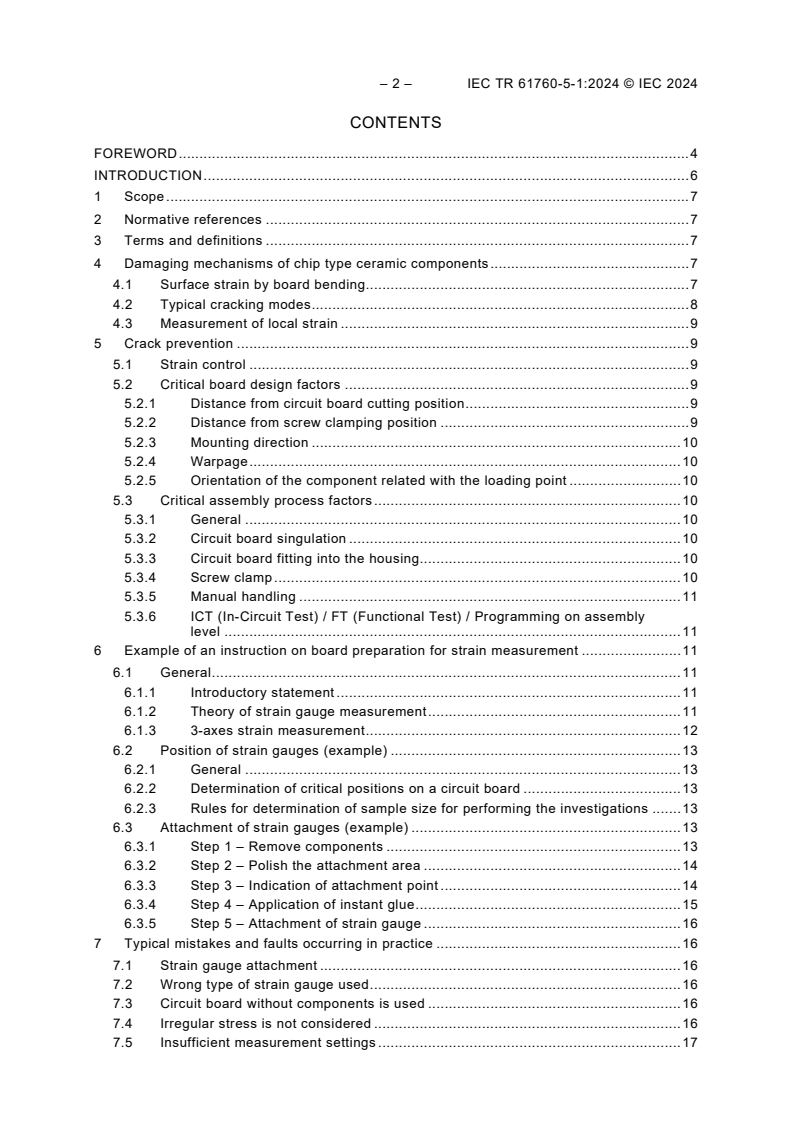
– 2 – IEC TR 61760-5-1:2024 © IEC 2024
CONTENTS
FOREWORD . 4
INTRODUCTION . 6
1 Scope . 7
2 Normative references . 7
3 Terms and definitions . 7
4 Damaging mechanisms of chip type ceramic components . 7
4.1 Surface strain by board bending. 7
4.2 Typical cracking modes . 8
4.3 Measurement of local strain . 9
5 Crack prevention . 9
5.1 Strain control . 9
5.2 Critical board design factors . 9
5.2.1 Distance from circuit board cutting position . 9
5.2.2 Distance from screw clamping position . 9
5.2.3 Mounting direction . 10
5.2.4 Warpage . 10
5.2.5 Orientation of the component related with the loading point . 10
5.3 Critical assembly process factors . 10
5.3.1 General . 10
5.3.2 Circuit board singulation . 10
5.3.3 Circuit board fitting into the housing. 10
5.3.4 Screw clamp . 10
5.3.5 Manual handling . 11
5.3.6 ICT (In-Circuit Test) / FT (Functional Test) / Programming on assembly
level . 11
6 Example of an instruction on board preparation for strain measurement . 11
6.1 General . 11
6.1.1 Introductory statement . 11
6.1.2 Theory of strain gauge measurement . 11
6.1.3 3-axes strain measurement . 12
6.2 Position of strain gauges (example) . 13
6.2.1 General . 13
6.2.2 Determination of critical positions on a circuit board . 13
6.2.3 Rules for determination of sample size for performing the investigations . 13
6.3 Attachment of strain gauges (example) . 13
6.3.1 Step 1 – Remove components . 13
6.3.2 Step 2 – Polish the attachment area . 14
6.3.3 Step 3 – Indication of attachment point . 14
6.3.4 Step 4 – Application of instant glue . 15
6.3.5 Step 5 – Attachment of strain gauge . 16
7 Typical mistakes and faults occurring in practice . 16
7.1 Strain gauge attachment . 16
7.2 Wrong type of strain gauge used . 16
7.3 Circuit board without components is used . 16
7.4 Irregular stress is not considered . 16
7.5 Insufficient measurement settings . 17
8 Evaluation of data and report . 17
9 Assembly process control . 18
9.1 Machine/Process capability . 18
9.2 Machine maintenance . 18
Annex A (informative) Examples and relevant processes . 19
A.1 Typical measurement results – Press-fit operation, Example 1 . 19
A.2 Typical measurement results – Press-fit operation, Example 2 . 20
A.3 Typical measurement results – Housing assembly by screwing . 22
A.4 Typical critical processes . 23
Bibliography . 24
Figure 1 – Mechanical stress by board bending . 8
Figure 2 – Strain simulation . 8
Figure 3 – Typical bending crack at a ceramic capacitor . 8
Figure 4 – Longitudinal stress . 8
Figure 5 – Diagonal stress . 9
Figure 6 – Strain control and bending strength . 9
Figure 7 – Strain during screwing . 11
Figure 8 – Resistor bridge for strain measurement . 12
Figure 9 – 3-axes strain gauge and maximum principle strain . 12
Figure 10 – De-soldering of components . 14
Figure 11 – Polishing the attachment area . 14
Figure 12 – Marking of the attachment point . 14
Figure 13 – Application of glue by transfer from polyethylene sheet . 15
Figure 14 – Direct application of glue . 15
Figure A.1 – Dosing control unit for exhaust treatment system equipped with a
connector using compliant press-fit technology . 19
Figure A.2 – Top and bottom side of circuit assembly of dosing control unit with strain
gauges replacing passive multilayer chip capacitors . 19
Figure A.3 – Strain measurement evolution for the different strain gauges during the
press-in process . 20
Figure A.4 – Press fit – Strain measurements using different strain gauges and
positions . 21
Figure A.5 – Screwing – Strain measurements using different strain gauges and
positions . 22
Table A.1 – Strain measurement results with different gauges and placements . 21
Table A.2 – Strain measurement results with different gauges and placements . 22
– 4 – IEC TR 61760-5-1:2024 © IEC 2024
INTERNATIONAL ELECTROTECHNICAL COMMISSION
____________
SURFACE MOUNTING TECHNOLOGY –
Part 5-1: Surface strain on circuit boards –
Strain gauge measurement applied to chip components
FOREWORD
1) The International Electrotechnical Commission (IEC) is a worldwide organization for standardization comprising
all national electrotechnical committees (IEC National Committees). The object of IEC is to promote international
co-operation on all questions concerning standardization in the electrical and electronic fields. To this end and
in addition to other activities, IEC publishes International Standards, Technical Specifications, Technical Reports,
Publicly Available Specifications (PAS) and Guides (hereafter referred to as “IEC Publication(s)”). Their
preparation is entrusted to technical committees; any IEC National Committee interested in the subject dealt with
may participate in this preparatory work. International, governmental and non-governmental organizations liaising
with the IEC also participate in this preparation. IEC collaborates closely with the International Organization for
Standardization (ISO) in accordance with conditions determined by agreement between the two organizations.
2) The formal decisions or agreements of IEC on technical matters express, as nearly as possible, an international
consensus of opinion on the relevant subjects since each technical committee has representation from all
interested IEC National Committees.
3) IEC Publications have the form of recommendations for international use and are accepted by IEC National
Committees in that sense. While all reasonable efforts are made to ensure that the technical content of IEC
Publications is accurate, IEC cannot be held responsible for the way in which they are used or for any
misinterpretation by any end user.
4) In order to promote international uniformity, IEC National Committees undertake to apply IEC Publications
transparently to the maximum extent possible in their national and regional publications. Any divergence between
any IEC Publication and the corresponding national or regional publication shall be clearly indicated in the latter.
5) IEC itself does not provide any attestation of conformity. Independent certification bodies provide conformity
assessment services and, in some areas, access to IEC marks of conformity. IEC is not responsible for any
services carried out by independent certification bodies.
6) All users should ensure that they have the latest edition of this publication.
7) No liability shall attach to IEC or its directors, employees, servants or agents including individual experts and
members of its technical committees and IEC National Committees for any personal injury, property damage or
other damage of any nature whatsoever, whether direct or indirect, or for costs (including legal fees) and
expenses arising out of the publication, use of, or reliance upon, this IEC Publication or any other IEC
Publications.
8) Attention is drawn to the Normative references cited in this publication. Use of the referenced publications is
indispensable for the correct application of this publication.
9) IEC draws attention to the possibility that the implementation of this document may involve the use of (a)
patent(s). IEC takes no position concerning the evidence, validity or applicability of any claimed patent rights in
respect thereof. As of the date of publication of this document, IEC had not received notice of (a) patent(s), which
may be required to implement this document. However, implementers are cautioned that this may not represent
the latest information, which may be obtained from the patent database available at https://patents.iec.ch. IEC
shall not be held responsible for identifying any or all such patent rights.
IEC TR 61760-5-1 has been prepared by IEC technical committee 91: Electronics assembly
technology. It is a Technical Report.
The text of this Technical Report is based on the following documents:
Draft Report on voting
91/1915/DTR 91/1927/RVDTR
Full information on the voting for its approval can be found in the report on voting indicated in
the above table.
The language used for the development of this Technical Report is English.
This document was drafted in accordance with ISO/IEC Directives, Part 2, and developed in
accordance with ISO/IEC Directives, Part 1 and ISO/IEC Directives, IEC Supplement, available
at www.iec.ch/members_experts/refdocs. The main document types developed by IEC are
described in greater detail at www.iec.ch/standardsdev/publications.
A list of all parts in the IEC 61760 series, published under the general title Surface mounting
technology, can be found on the IEC website.
The committee has decided that the contents of this document will remain unchanged until the
stability date indicated on the IEC website under webstore.iec.ch in the data related to the
specific document. At this date, the document will be
• reconfirmed,
• withdrawn, or
• revised.
IMPORTANT – The "colour inside" logo on the cover page of this document indicates
that it contains colours which are considered to be useful for the correct understanding
of its contents. Users should therefore print this document using a colour printer.
– 6 – IEC TR 61760-5-1:2024 © IEC 2024
INTRODUCTION
This Technical Report applies to electronic and electromechanical circuit board assemblies and
describes current best-practices for dealing with mechanical stress induced cracks in the body
of surface-mount ceramic components soldered onto circuit boards.
Circuit boards are becoming smaller and thinner, design margins are decreasing, and
components are becoming more sensitive to mechanical stresses. In consequence in-depth
strain control on a circuit board is getting more and more important to prevent mechanical
damage to components.
This Technical Report is an informative document which serves to illustrate the technically
feasible options and provides a basis for customer and supplier discussions and agreements.
It is based on many years of experience of component manufacturers and users in measuring
surface strain on circuit board surfaces during various assembly processes. It is not intended
to be regarded as a specification or standard. Formulations and data expressed in the form of
provision such as requirements or recommendations do not claim to be provisions and are just
suggested as the results of the discussion.
Related standards are gathered in the bibliography.
SURFACE MOUNTING TECHNOLOGY –
Part 5-1: Surface strain on circuit boards –
Strain gauge measurement applied to chip components
1 Scope
This document describes examples of methods using electrical strain gauges for determination
of critical mechanical stresses in assembly processes. These stresses can damage chip type
ceramic components, causing so called “bending cracks”. Area-array components are excluded
from the scope of this document.
2 Normative references
There are no normative references in this document.
3 Terms and definitions
For the purposes of this document, the terms and definitions given in IEC 60194-2 and the
following apply.
ISO and IEC maintain terminological databases for use in standardization at the following
addresses:
• IEC Electropedia: available at https://www.electropedia.org/
• ISO Online browsing platform: available at https://www.iso.org/obp
3.1
principal strain
maximum and minimum normal strains in a plane, always perpendicular to each other and
oriented in directions for which the shear strains are zero
3.2
maximum principal strain
maximum value of principal strain developed in the component body
Note 1 to entry: Failure of a material or component will occur when the maximum principal strain developed in the
body exceeds the limiting value of strain for a certain component.
4 Damaging mechanisms of chip type ceramic components
4.1 Surface strain by board bending
When a board is bent, lands are pulled outwards and generate mechanical stress on the solder-
joints, electrodes or components (Figure 1, Figure 2). This mechanical stress causes defects,
for example a bending crack in a ceramic capacitor (Figure 3). The root cause of this defect is
the local strain at the surface on which the component is mounted.
– 8 – IEC TR 61760-5-1:2024 © IEC 2024
Figure 1 – Mechanical stress by board bending
Reproduced with the permission of Murata Manufacturing
Figure 2 – Strain simulation
Reproduced with the permission of Murata Manufacturing
Figure 3 – Typical bending crack at a ceramic capacitor
4.2 Typical cracking modes
Bending stress can occur in any direction, see Figure 4 and Figure 5. The cracks were made
visible by grinding from the board side. The position and shape of cracks can be used to
estimate the direction of stress. The local strain at the position at which the component is
mounted causes the cracks. Therefore, even if a board does not look bent, this defect could
occur by local surface stress or short time impact.
Reproduced with the permission of Murata Manufacturing
Figure 4 – Longitudinal stress
Reproduced with the permission of Murata Manufacturing
Figure 5 – Diagonal stress
4.3 Measurement of local strain
Local strains can occur in any direction, see Figure 4 and Figure 5. 3-axes strain gauges
provide a full assessment of the strain state. The use of 1-axis or 2-axes measurements
provides limited information on the strain state.
5 Crack prevention
5.1 Strain control
To prevent bending cracks described in 4.1 and 4.2, strain control on a PCB is needed. The
bending strength of SMD for example can be determined by the so-called substrate bending
test, as provided in IEC 60068-2-21. However, the real mechanical strength of a surface mount
component depends on various design and process factors (e.g. land size, solder quantity/type,
PCB material/type, Cu foil thickness, strain rate, etc.). Furthermore, considering the strain
measurement accuracy, measurement repeatability, and irregular stresses in assembly
processes, a certain safety margin is needed, see Figure 6.
Figure 6 – Strain control and bending strength
5.2 Critical board design factors
5.2.1 Distance from circuit board cutting position
Components mounted close to a cutting or singulation position are at risk. A slit can reduce the
cutting stress if it is placed between the component and the cutting line. Also, a deep v-groove
can reduce the cutting stress.
5.2.2 Distance from screw clamping position
Components mounted close to a screw clamping position are at risk.
– 10 – IEC TR 61760-5-1:2024 © IEC 2024
5.2.3 Mounting direction
Risk can be reduced, if a components’ longitudinal axis is oriented perpendicular to the
maximum principle strain.
5.2.4 Warpage
Warpage can be the cause of surface stress when a circuit board is flattened when fitted into
the housing.
5.2.5 Orientation of the component related with the loading point
The mechanical load to components is influenced by their orientation relative to the forces
applied to the board.
5.3 Critical assembly process factors
5.3.1 General
In general, an assessment of all processes which involve mechanical loads applied to populated
circuit boards is needed. This implies that such an assessment needs to start after the first
reflow cycle. All process steps, including solder paste printing for the second reflow side (top
side), conveyor movement, pick-and-place etc. occurring after the first reflow cycle need to be
considered. Further information on suc
...


Questions, Comments and Discussion
Ask us and Technical Secretary will try to provide an answer. You can facilitate discussion about the standard in here.
Loading comments...