ASTM E2642-09(2021)
(Terminology)Standard Terminology for Scientific Charge-Coupled Device (CCD) Detectors
Standard Terminology for Scientific Charge-Coupled Device (CCD) Detectors
SIGNIFICANCE AND USE
3.1 This terminology was drafted to exclude any commercial relevance to any one vendor by using only general terms that are acknowledged by all vendors and should be revised as charge-coupled device (CCD) technology matures. This terminology uses standard explanations, symbols, and abbreviations.
SCOPE
1.1 This terminology brings together and clarifies the basic terms and definitions used with scientific grade cooled charge-coupled device (CCD) detectors, thus allowing end users and vendors to use common documented terminology when evaluating or discussing these instruments. CCD detectors are sensitive to light in the region from 200 nm to 1100 nm and the terminology outlined in the document is based on the detection technology developed around CCDs for this range of the spectrum.
1.2 The values stated in SI units are to be regarded as standard. No other units of measurement are included in this standard.
1.3 This international standard was developed in accordance with internationally recognized principles on standardization established in the Decision on Principles for the Development of International Standards, Guides and Recommendations issued by the World Trade Organization Technical Barriers to Trade (TBT) Committee.
General Information
- Status
- Published
- Publication Date
- 31-Aug-2021
- Technical Committee
- E13 - Molecular Spectroscopy and Separation Science
- Drafting Committee
- E13.08 - Raman Spectroscopy
Relations
- Effective Date
- 01-Mar-2010
- Effective Date
- 01-Sep-2005
- Effective Date
- 10-Sep-2002
- Effective Date
- 10-Sep-2000
Overview
ASTM E2642-09(2021): Standard Terminology for Scientific Charge-Coupled Device (CCD) Detectors establishes a unified vocabulary for cooled scientific-grade CCD detectors. Created by ASTM, this internationally recognized standard clarifies core terms, definitions, symbols, and abbreviations used in CCD detector technology. By providing a common language, the standard facilitates effective communication between end users and manufacturers, especially when specifying, evaluating, or discussing instrument performance. This standard focuses exclusively on general, vendor-neutral terminology to support broad application across the scientific community.
Key Topics
- Foundational CCD Terms: The document defines central terms related to the design, operation, and performance of cooled scientific CCD detectors, such as charge-coupled device, pixel, binning, quantum efficiency (QE), and signal-to-noise ratio (SNR).
- Architecture and Signal Processing: The standard covers diverse CCD architectures, including front-illuminated, back-illuminated, frame-transfer, and electron-multiplying CCDs. It explains signal processing elements like analog-to-digital (A/D) conversion, output amplifiers, and readout techniques.
- Performance Characteristics: Key definitions include dynamic range, dark current, dark noise, read noise, charge transfer efficiency (CTE), exposure time, and pixel non-uniformity.
- Operational Modes and Enhancements: The terminology addresses advanced operational methods (e.g., advanced inverted mode operation/AIMO, multi-pinned phase operation/MPP), spectral sensitivity enhancements (such as deep depletion and antireflective coatings), and system noise sources.
- Materials and Cooling Techniques: The standard explains materials like silicon and indium tin oxide, and cooling technologies such as Peltier and thermoelectric cooling that improve dark current performance.
- Unit Standards: Values are standardized in SI units only, ensuring global consistency.
- International Compliance: Developed in line with the World Trade Organization’s TBT Committee principles, reinforcing its global relevance.
Applications
ASTM E2642-09(2021) terminology is vital for:
- Scientific Instrumentation: Standardized terminology aids in specifying, comparing, and procuring scientific-grade cooled CCD detectors for spectroscopy, imaging, and analytical instrumentation.
- Quality Assurance and Product Development: Ensures consistent understanding and reporting of performance metrics between vendors and laboratories, essential for quality control and R&D.
- Cross-disciplinary Collaboration: Facilitates efficient communication across various scientific domains-such as molecular spectroscopy, astronomy, and materials science-where CCD detectors are integral to data acquisition.
- Training and Documentation: Provides an authoritative reference for technical documentation, education, and training materials, ensuring new users or stakeholders understand essential CCD concepts.
- Regulatory and Procurement Processes: The internationally recognized, vendor-neutral language minimizes interpretation errors and promotes harmonized procurement and compliance procedures worldwide.
Related Standards
- ASTM E131: Terminology Relating to Molecular Spectroscopy - Provides foundational terms that complement CCD terminology, especially in analytical contexts.
- Other Imaging Sensor Standards: Standards addressing complementary metal oxide semiconductor (CMOS) detectors or other imaging technologies may be referenced for broader context.
- World Trade Organization TBT Principles: Ensures that terminology aligns with international guidelines on standardization and trade.
By using ASTM E2642-09(2021), organizations and professionals ensure clarity, reduce ambiguity, and foster innovation in scientific CCD detection and imaging technology. This terminology standard is an essential resource for anyone engaged in the specification, application, or advancement of CCD detector systems.
Buy Documents
ASTM E2642-09(2021) - Standard Terminology for Scientific Charge-Coupled Device (CCD) Detectors
Frequently Asked Questions
ASTM E2642-09(2021) is a standard published by ASTM International. Its full title is "Standard Terminology for Scientific Charge-Coupled Device (CCD) Detectors". This standard covers: SIGNIFICANCE AND USE 3.1 This terminology was drafted to exclude any commercial relevance to any one vendor by using only general terms that are acknowledged by all vendors and should be revised as charge-coupled device (CCD) technology matures. This terminology uses standard explanations, symbols, and abbreviations. SCOPE 1.1 This terminology brings together and clarifies the basic terms and definitions used with scientific grade cooled charge-coupled device (CCD) detectors, thus allowing end users and vendors to use common documented terminology when evaluating or discussing these instruments. CCD detectors are sensitive to light in the region from 200 nm to 1100 nm and the terminology outlined in the document is based on the detection technology developed around CCDs for this range of the spectrum. 1.2 The values stated in SI units are to be regarded as standard. No other units of measurement are included in this standard. 1.3 This international standard was developed in accordance with internationally recognized principles on standardization established in the Decision on Principles for the Development of International Standards, Guides and Recommendations issued by the World Trade Organization Technical Barriers to Trade (TBT) Committee.
SIGNIFICANCE AND USE 3.1 This terminology was drafted to exclude any commercial relevance to any one vendor by using only general terms that are acknowledged by all vendors and should be revised as charge-coupled device (CCD) technology matures. This terminology uses standard explanations, symbols, and abbreviations. SCOPE 1.1 This terminology brings together and clarifies the basic terms and definitions used with scientific grade cooled charge-coupled device (CCD) detectors, thus allowing end users and vendors to use common documented terminology when evaluating or discussing these instruments. CCD detectors are sensitive to light in the region from 200 nm to 1100 nm and the terminology outlined in the document is based on the detection technology developed around CCDs for this range of the spectrum. 1.2 The values stated in SI units are to be regarded as standard. No other units of measurement are included in this standard. 1.3 This international standard was developed in accordance with internationally recognized principles on standardization established in the Decision on Principles for the Development of International Standards, Guides and Recommendations issued by the World Trade Organization Technical Barriers to Trade (TBT) Committee.
ASTM E2642-09(2021) is classified under the following ICS (International Classification for Standards) categories: 01.040.37 - Image technology (Vocabularies); 37.020 - Optical equipment. The ICS classification helps identify the subject area and facilitates finding related standards.
ASTM E2642-09(2021) has the following relationships with other standards: It is inter standard links to ASTM E131-10, ASTM E131-05, ASTM E131-02, ASTM E131-00a. Understanding these relationships helps ensure you are using the most current and applicable version of the standard.
ASTM E2642-09(2021) is available in PDF format for immediate download after purchase. The document can be added to your cart and obtained through the secure checkout process. Digital delivery ensures instant access to the complete standard document.
Standards Content (Sample)
This international standard was developed in accordance with internationally recognized principles on standardization established in the Decision on Principles for the
Development of International Standards, Guides and Recommendations issued by the World Trade Organization Technical Barriers to Trade (TBT) Committee.
Designation:E2642 −09 (Reapproved 2021)
Standard Terminology for
Scientific Charge-Coupled Device (CCD) Detectors
This standard is issued under the fixed designation E2642; the number immediately following the designation indicates the year of
original adoption or, in the case of revision, the year of last revision.Anumber in parentheses indicates the year of last reapproval.A
superscript epsilon (´) indicates an editorial change since the last revision or reapproval.
1. Scope advanced inverted mode operation (AIMO), n—a commer-
cial tradename given to a method of reducing the rate of
1.1 This terminology brings together and clarifies the basic
generation of dark current. Also known as multi-pinned
terms and definitions used with scientific grade cooled charge-
phase operation.
coupled device (CCD) detectors, thus allowing end users and
vendors to use common documented terminology when evalu-
analog-to-digital (A/D) converter, n—an electronic circuitry
ating or discussing these instruments. CCD detectors are
in a CCD detector that converts an analog signal into digital
sensitivetolightintheregionfrom200nmto1100nmandthe
values, which are specified in terms of bits that can be
terminologyoutlinedinthedocumentisbasedonthedetection
manipulated by the computer.
technology developed around CCDs for this range of the
anti-blooming structure, n—a structure built into the pixel to
spectrum.
prevent signal charge above full-well capacity from bloom-
1.2 The values stated in SI units are to be regarded as
ing into adjacent pixels.
standard. No other units of measurement are included in this
DISCUSSION—Anti-blooming structures bleed off any excess charge
standard.
before they can overflow the pixel and thereby stop blooming. These
structures can reduce the effective quantum efficiency and introduce
1.3 This international standard was developed in accor-
nonlinearity into the sensor.
dance with internationally recognized principles on standard-
ization established in the Decision on Principles for the
antireflective (AR) coating, n—a coating applied to either the
Development of International Standards, Guides and Recom-
frontsurfaceoftheCCDorthevacuumwindowsurfaces,to
mendations issued by the World Trade Organization Technical
minimizetheamountofreflectedenergy(orelectromagnetic
Barriers to Trade (TBT) Committee.
radiation) so as to maximize the amount of transmitted
energy.
2. Referenced Documents
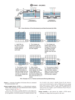
2 back-illuminated CCD (BI CCD), n—atypeofCCDthathas
2.1 ASTM Standards:
been uniformly reduced in thickness on the side away from
E131Terminology Relating to Molecular Spectroscopy
the gate structure (see Fig. 1b) and positioned such that the
photons are detected on that side.
3. Significance and Use
DISCUSSION—A BI CCD leads to an improvement in sensitivity to
3.1 This terminology was drafted to exclude any commer-
incoming photons from the soft X-ray to the near-infrared (NIR)
cial relevance to any one vendor by using only general terms
regions of the spectrum with the highest response in the visible region.
that are acknowledged by all vendors and should be revised as
However, compared to a front-illuminated CCD, it suffers from higher
charge-coupled device (CCD) technology matures.This termi- dark currents and interference fringe formation (etaloning) usually in
the NIR region. Also called back-thinned CCD.
nologyusesstandardexplanations,symbols,andabbreviations.
binning, n—the process of combining charge from adjacent
4. Terminology
pixels in a CCD prior to read out.
4.1 Definitions:
DISCUSSION—There are two main types of binning: (1) vertical
binningand (2)horizontalbinning(seeFig.2).Summingchargeonthe
CCD and doing a single readout results in better noise performance
This terminology is under the jurisdiction of ASTM Committee E13 on thanreadingoutseveralpixelsandthensummingtheminthecomputer
Molecular Spectroscopy and Separation Science and is the direct responsibility of
memory. This is because each act of reading out contributes to noise
Subcommittee E13.08 on Raman Spectroscopy.
(see noise).
Current edition approved Sept. 1, 2021. Published September 2021. Originally
approved in 2008. Last previous edition approved in 2015 as E2642–09 (2015).
CCD bias, n—the minimum analog offset added to the signal
DOI: 10.1520/E2642-09R21.
before the A/D converter to ensure a positive digital output
For referenced ASTM standards, visit the ASTM website, www.astm.org, or
each time a signal is read out.
contact ASTM Customer Service at service@astm.org. For Annual Book of ASTM
DISCUSSION—The CCD bias is set at the time of manufacture and
Standards volume information, refer to the standard’s Document Summary page on
the ASTM website. remains set over the lifetime of the camera.
Copyright © ASTM International, 100 Barr Harbor Drive, PO Box C700, West Conshohocken, PA 19428-2959. United States
E2642−09 (2021)
FIG. 1Cross Sections of Front-Illuminated (a) and Back-Illuminated (b) CCDs
FIG. 2Example of a 2×2 Vertical and Horizontal Binning Methodology
size of pixels in the sensor is typically 26µm×26 µm; however,
charge, n—measure of number of electrons that are contained
sensorscanbemanufacturedinavarietyofdifferentpixelsizesranging
in a pixel potential well.
from 6µm×6 µm to 50µm×50 µm. Although mathematically
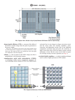
charge-coupled device (CCD), n—a silicon-based semicon-
incorrect, the dimension unit of a square pixel is typically given in
ductor chip consisting of a two-dimensional matrix of photo square microns (for example, a pixel of dimension 26µm×26 µm is
specified as 26×26µm ).
sensors or pixels (see Fig. 3).
DISCUSSION—The matrix is usually referred to as the image area.
charge transfer, n—the process by which a CCD moves
Electronic charge is accumulated on the image area and transferred out
by the application of electrical potentials to shielded electrodes. The electrons or charge from one pixel to the next.
E2642−09 (2021)
FIG. 3Typical 1024×256 (26×26 µm pixel) Element CCD Sensor Used for Spectroscopy
charge transfer efficiency (CTE), n—measureoftheabilityof each pixel has its own charge-to-voltage conversion circuit,
the CCD to transfer charge from the point of generation to and the sensor often also includes amplifiers, noise-
the device output.
correction, and digitization circuits. Due to the additional
DISCUSSION—Itisdefinedasthefractionofthechargeinitiallystored
components associated with each pixel, the sensitivity to
in a CCD element that is transferred to an adjacent element by a single
light is lower than with a CCD, the signal is noisier, and the
clock cycle. The value for CTE is not constant but varies with signal
uniformity is lower. But the sensor can be built to require
size, temperature, and clock frequency.
less off-chip circuitry for basic operation (see Fig. 4).
column, n—a line of pixels in the CCD’s image area that is
perpendicular to the horizontal register. correlated double sampling, n—areadoutsamplingtechnique
used to achieve higher precision in CCD readout.
complementary metal oxide semiconductor (CMOS),
n—technology widely used to manufacture electronic de-
vicesandimagesensorssimilartoCCDs.InaCMOSsensor,
FIG. 4Typical Architectures of CCD and CMOS Sensors
E2642−09 (2021)
DISCUSSION—Thesamplingcircuitissettoapredeterminedreference DISCUSSION—A true 16-bit detector will have a dynamic range of
level and then the actual pixel voltage is sampled in order to find the 65535:1.
difference between the two. The resulting correlation minimizes read
electron-multiplying CCD (EMCCD), n—type of CCD that
noise, especially in ultra-low-noise CCD detectors.
has a two-way readout register, that is, the shift register and
cosmic event, n—a spurious signal caused by a cosmic ray or
the gain register, each with its own output amplifier. When
particle hitting the CCD sensor. It is typically observed to
the charge is read out through the shift register, the detector
resultinahighintensitysignalcomingfromasinglepixelor
works like a standard CCD detector, and when the charge is
small group of pixels.
read out through the gain register, it undergoes charge
dark current, n—a current that occurs naturally through the amplification as a result of a different electrode structure
embedded underneath the pixels of this register (see Fig. 6).
thermally generated electrons in the semiconductor material
of the CCD. It is intrinsic to semiconductors and is indepen-
DISCUSSION—Passing charge through the gain register allows the
signal to be amplified before readout noise is added at the readout
dent of incident photons.
amplifier, thus improving the signal-to-noise ratios making the camera
DISCUSSION—DarkcurrentisdependantontheCCD’stemperature.It
highly sensitive in the low-light regime.
is expressed in electrons/pixel/unit time.
dark noise, n—the shot noise associated with the dark current
etaloning, n—a phenomenon by which constructive and de-
for the given exposure time, and is approximately equal to
structive interference fringes are produced in a back-
the square root of the dark current times the exposure time
illuminated CCD caused by internal reflections between the
used.Itisusuallyexpressedintermsofnumberofelectrons.
two parallel surfaces of the CCD. Typically BI CCDs
experience etaloning effects when subjected to NIR signals
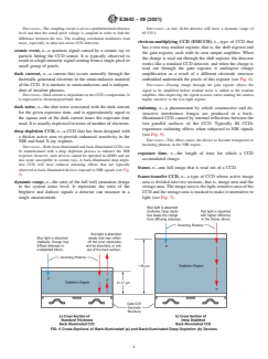
deep depletion CCD, n—a CCD that has been designed with
(see Fig. 5).
a thicker active area to provide enhanced sensitivity in the
DISCUSSION—This effect causes the device to become transparent to
NIR and hard X-ray regimes.
incoming photons in the NIR region.
DISCUSSION—Both front-illuminated and back-illuminated CCDs can
be manufactured with a deep depletion process to enhance the NIR
exposure time, n—the length of time for which a CCD
response; however, such devices cannot be operated in AIMO and are
accumulated charge.
also more susceptible to cosmic rays. A back-illuminated deep deple-
tion CCD will have reduced etaloning effects that are typically
frame, n—one full image that is read out of a CCD.
observed in back-illuminated devices exposed to NIR signals (see Fig.
5).
frame-transfer CCD, n—a type of CCD whose active image
dynamic range, n—the ratio of the full well saturation charge area is divided into two sections, that is, image area and the
storagearea.Theimageareaisthelightsensitiveareaofthe
to the system noise level. It represents the ratio of the
brightest and darkest signals a detector can measure in a CCDandthestorageareaismaskedtomakeitinsensitiveto
light (see Fig. 7).
single measurement.
FIG. 5Cross-Sections of Back-Illuminated (a) and Back-Illuminated Deep Depletion (b) Devices
E2642−09 (2021)
FIG. 6Typical Sketch of Full-Frame EMCCD Sensor
FIG. 7Typical Sketch of a Frame-Transfer CCD
DISCUSSION—During operation the charge accumulated in the image
full-frame CCD, n—a type of CCD that uses the entire silicon
section is rapidly transferred to the storage section at the end of the
active area for photon detection. A shutter is required to
exposure time. The storage area is then readout as the image section
eliminate image smear (see Fig. 3).
accumulateschargeforthenextexposure.ThistypeofCCDreducesor
eliminatestheneedforashutter,dependingonthespeedofthetransfer
full well capacity, n—the maximum number of photoelectrons
from image to storage.
thatcanbecollectedonasinglepixelintheimageareaorin
front-illuminated CCD (FI CCD), n—a type of CCD in the horizontal register of a CCD. It is typically specified in
which the photons are detected through the gate structure terms of number of e
...


Questions, Comments and Discussion
Ask us and Technical Secretary will try to provide an answer. You can facilitate discussion about the standard in here.
Loading comments...