ASTM F1192-11
(Guide)Standard Guide for the Measurement of Single Event Phenomena (SEP) Induced by Heavy Ion Irradiation of Semiconductor Devices
Standard Guide for the Measurement of Single Event Phenomena (SEP) Induced by Heavy Ion Irradiation of Semiconductor Devices
SIGNIFICANCE AND USE
Many modern integrated circuits, power transistors, and other devices experience SEP when exposed to cosmic rays in interplanetary space, in satellite orbits or during a short passage through trapped radiation belts. It is essential to be able to predict the SEP rate for a specific environment in order to establish proper techniques to counter the effects of such upsets in proposed systems. As the technology moves toward higher density ICs, the problem is likely to become even more acute.
This guide is intended to assist experimenters in performing ground tests to yield data enabling SEP predictions to be made.
SCOPE
1.1 This guide defines the requirements and procedures for testing integrated circuits and other devices for the effects of single event phenomena (SEP) induced by irradiation with heavy ions having an atomic number Z ≥ 2. This description specifically excludes the effects of neutrons, protons, and other lighter particles that may induce SEP via another mechanism. SEP includes any manifestation of upset induced by a single ion strike, including soft errors (one or more simultaneous reversible bit flips), hard errors (irreversible bit flips), latchup (persistent high conducting state), transients induced in combinatorial devices which may introduce a soft error in nearby circuits, power field effect transistor (FET) burn-out and gate rupture. This test may be considered to be destructive because it often involves the removal of device lids prior to irradiation. Bit flips are usually associated with digital devices and latchup is usually confined to bulk complementary metal oxide semiconductor, (CMOS) devices, but heavy ion induced SEP is also observed in combinatorial logic programmable read only memory, (PROMs), and certain linear devices that may respond to a heavy ion induced charge transient. Power transistors may be tested by the procedure called out in Method 1080 of MIL STD 750.
1.2 The procedures described here can be used to simulate and predict SEP arising from the natural space environment, including galactic cosmic rays, planetary trapped ions, and solar flares. The techniques do not, however, simulate heavy ion beam effects proposed for military programs. The end product of the test is a plot of the SEP cross section (the number of upsets per unit fluence) as a function of ion LET (linear energy transfer or ionization deposited along the ion's path through the semiconductor). This data can be combined with the system's heavy ion environment to estimate a system upset rate.
1.3 Although protons can cause SEP, they are not included in this guide. A separate guide addressing proton induced SEP is being considered.
1.4 The values stated in SI units are to be regarded as standard. No other units of measurement are included in this standard.
1.5 This standard does not purport to address all of the safety concerns, if any, associated with its use. It is the responsibility of the user of this standard to establish appropriate safety and health practices and determine the applicability of regulatory limitations prior to use.
General Information
Buy Standard
Standards Content (Sample)
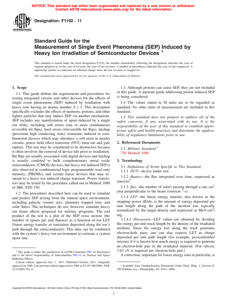
NOTICE: This standard has either been superseded and replaced by a new version or withdrawn.
Contact ASTM International (www.astm.org) for the latest information
Designation: F1192 − 11
Standard Guide for the
Measurement of Single Event Phenomena (SEP) Induced by
1
Heavy Ion Irradiation of Semiconductor Devices
This standard is issued under the fixed designation F1192; the number immediately following the designation indicates the year of
original adoption or, in the case of revision, the year of last revision. A number in parentheses indicates the year of last reapproval. A
superscript epsilon (´) indicates an editorial change since the last revision or reapproval.
This standard has been approved for use by agencies of the U.S. Department of Defense.
1. Scope 1.3 Although protons can cause SEP, they are not included
in this guide.Aseparate guide addressing proton induced SEP
1.1 This guide defines the requirements and procedures for
is being considered.
testing integrated circuits and other devices for the effects of
single event phenomena (SEP) induced by irradiation with 1.4 The values stated in SI units are to be regarded as
heavy ions having an atomic number Z ≥ 2. This description standard. No other units of measurement are included in this
specifically excludes the effects of neutrons, protons, and other standard.
lighter particles that may induce SEP via another mechanism.
1.5 This standard does not purport to address all of the
SEP includes any manifestation of upset induced by a single
safety concerns, if any, associated with its use. It is the
ion strike, including soft errors (one or more simultaneous
responsibility of the user of this standard to establish appro-
reversible bit flips), hard errors (irreversible bit flips), latchup
priate safety and health practices and determine the applica-
(persistent high conducting state), transients induced in com-
bility of regulatory limitations prior to use.
binatorial devices which may introduce a soft error in nearby
2. Referenced Documents
circuits, power field effect transistor (FET) burn-out and gate
2
rupture. This test may be considered to be destructive because
2.1 Military Standard:
it often involves the removal of device lids prior to irradiation.
750 Method 1080
Bit flips are usually associated with digital devices and latchup
is usually confined to bulk complementary metal oxide 3. Terminology
semiconductor,(CMOS)devices,butheavyioninducedSEPis
3.1 Definitions of Terms Specific to This Standard:
also observed in combinatorial logic programmable read only
3.1.1 DUT—device under test.
memory, (PROMs), and certain linear devices that may re-
3.1.2 fluence—the flux integrated over time, expressed as
spond to a heavy ion induced charge transient. Power transis-
2
ions/cm .
tors may be tested by the procedure called out in Method 1080
2
3.1.3 flux—the number of ions/s passing through a one cm
of MIL STD 750.
2
area perpendicular to the beam (ions/cm -s).
1.2 The procedures described here can be used to simulate
3.1.4 LET—the linear energy transfer, also known as the
and predict SEP arising from the natural space environment,
stopping power dE/dx, is the amount of energy deposited per
including galactic cosmic rays, planetary trapped ions, and
unit length along the path of the incident ion, typically
solar flares. The techniques do not, however, simulate heavy
2
normalized by the target density and expressed as MeV-cm /
ion beam effects proposed for military programs. The end
mg.
product of the test is a plot of the SEP cross section (the
3.1.4.1 Discussion—LET values are obtained by dividing
number of upsets per unit fluence) as a function of ion LET
the energy per unit track length by the density of the irradiated
(linear energy transfer or ionization deposited along the ion’s
medium. Since the energy lost along the track generates
path through the semiconductor). This data can be combined
electron-hole pairs, one can also express LET as charge
with the system’s heavy ion environment to estimate a system
deposited per unit path length (for example, picocoulombs/
upset rate.
micron) if it is known how much energy is required to generate
an electron-hole pair in the irradiated material. (For silicon,
1 3.62 eV is required per electron-hole pair.)
This guide is under the jurisdiction of ASTM Committee F01 on Electronics
and is the direct responsibility of Subcommittee F01.11 on Nuclear and Space Acorrection,importantforlowerenergyionsinparticular,is
Radiation Effects.
Current edition approved Oct. 1, 2011. Published October 2011. Originally
2
approvedin1988.Lastpreviouseditionapprovedin2006asF1192–00(2006).DOI: Available from Standardization Documents Order Desk, Bldg. 4, Section D,
10.1520/F1192-11. 700 Robbins Ave., Philadelphia, PA 19111–5094.
Copyright © ASTM International, 100 Barr Harbor Drive, PO Box C700, West Conshohocken, PA 19428-2959. United States
1
---------------------- Page: 1 ----------------------
F1192 − 11
made to allow for the loss of ion
...
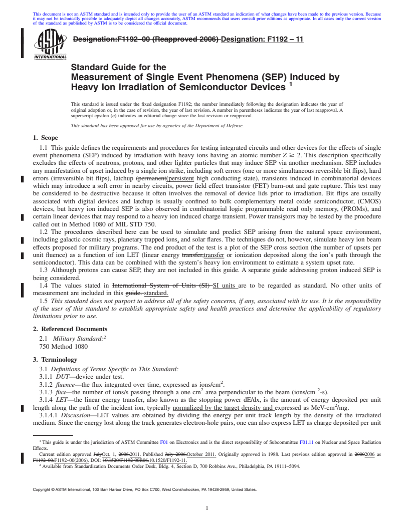
This document is not anASTM standard and is intended only to provide the user of anASTM standard an indication of what changes have been made to the previous version. Because
it may not be technically possible to adequately depict all changes accurately, ASTM recommends that users consult prior editions as appropriate. In all cases only the current version
of the standard as published by ASTM is to be considered the official document.
Designation:F1192–00 (Reapproved 2006) Designation:F1192–11
Standard Guide for the
Measurement of Single Event Phenomena (SEP) Induced by
1
Heavy Ion Irradiation of Semiconductor Devices
This standard is issued under the fixed designation F1192; the number immediately following the designation indicates the year of
original adoption or, in the case of revision, the year of last revision. A number in parentheses indicates the year of last reapproval. A
superscript epsilon (´) indicates an editorial change since the last revision or reapproval.
This standard has been approved for use by agencies of the Department of Defense.
1. Scope
1.1 This guide defines the requirements and procedures for testing integrated circuits and other devices for the effects of single
event phenomena (SEP) induced by irradiation with heavy ions having an atomic number Z$ 2. This description specifically
excludes the effects of neutrons, protons, and other lighter particles that may induce SEP via another mechanism. SEP includes
any manifestation of upset induced by a single ion strike, including soft errors (one or more simultaneous reversible bit flips), hard
errors (irreversible bit flips), latchup (permanent(persistent high conducting state), transients induced in combinatorial devices
which may introduce a soft error in nearby circuits, power field effect transistor (FET) burn-out and gate rupture. This test may
be considered to be destructive because it often involves the removal of device lids prior to irradiation. Bit flips are usually
associated with digital devices and latchup is usually confined to bulk complementary metal oxide semiconductor, (CMOS)
devices, but heavy ion induced SEP is also observed in combinatorial logic programmable read only memory, (PROMs), and
certain linear devices that may respond to a heavy ion induced charge transient. Power transistors may be tested by the procedure
called out in Method 1080 of MIL STD 750.
1.2 The procedures described here can be used to simulate and predict SEP arising from the natural space environment,
including galactic cosmic rays, planetary trapped ions, and solar flares. The techniques do not, however, simulate heavy ion beam
effects proposed for military programs. The end product of the test is a plot of the SEP cross section (the number of upsets per
unit fluence) as a function of ion LET (linear energy transfer,transfer or ionization deposited along the ion’s path through the
semiconductor). This data can be combined with the system’s heavy ion environment to estimate a system upset rate.
1.3 Although protons can cause SEP, they are not included in this guide. A separate guide addressing proton induced SEP is
being considered.
1.4 The values stated in International System of Units (SI) SI units are to be regarded as standard. No other units of
measurement are included in this guide. standard.
1.5 This standard does not purport to address all of the safety concerns, if any, associated with its use. It is the responsibility
of the user of this standard to establish appropriate safety and health practices and determine the applicability of regulatory
limitations prior to use.
2. Referenced Documents
2
2.1 Military Standard:
750 Method 1080
3. Terminology
3.1 Definitions of Terms Specific to This Standard:
3.1.1 DUT—device under test.
2
3.1.2 fluence—the flux integrated over time, expressed as ions/cm .
2 2
3.1.3 flux—the number of ions/s passing through a one cm area perpendicular to the beam (ions/cm -s).
3.1.4 LET—the linear energy transfer, also known as the stopping power dE/dx, is the amount of energy deposited per unit
2
length along the path of the incident ion, typically normalized by the target density and expressed as MeV-cm /mg.
3.1.4.1 Discussion—LET values are obtained by dividing the energy per unit track length by the density of the irradiated
medium. Since the energy lost along the track generates electron-hole pairs, one can also express LETas charge deposited per unit
1
This guide is under the jurisdiction of ASTM Committee F01 on Electronics and is the direct responsibility of Subcommittee F01.11 on Nuclear and Space Radiation
Effects.
Current edition approved JulyOct. 1, 2006.2011. Published July 2006.October 2011. Originally approved in 1988. Last previous edition approved in 20002006 as
F1192–00.F1192–00(2006). DOI: 10.1520/F1192-00R06.10.1520/F1192-11.
2
Available from Standardization Documents Order Desk, Bldg. 4, Section D, 700 Robbins Ave., Philadelphia, PA 19111–5094.
Copyright © ASTM International, 100 Barr Harbor Drive, PO
...


Questions, Comments and Discussion
Ask us and Technical Secretary will try to provide an answer. You can facilitate discussion about the standard in here.