ISO 19606:2017
(Main)Fine ceramics (advanced ceramics, advanced technical ceramics) — Test method for surface roughness of fine ceramic films by atomic force microscopy
Fine ceramics (advanced ceramics, advanced technical ceramics) — Test method for surface roughness of fine ceramic films by atomic force microscopy
ISO 19606:2017 describes a method to evaluate the adequateness of a probe tip for fine-ceramic thin-film surface roughness measurements by atomic force microscopy, of surfaces with an arithmetical mean roughness, Ra, in the range of about 1 nm to 30 nm and a mean width of roughness profile elements, RSm, in the range of about 0,04 μm to 2,5 μm.
Céramiques techniques — Méthode d'essai pour la rugosité de surface des films céramique fins par microscopie à force atomique
General Information
- Status
- Withdrawn
- Publication Date
- 12-Jan-2017
- Technical Committee
- ISO/TC 206 - Fine ceramics
- Drafting Committee
- ISO/TC 206/WG 10 - Coatings
- Current Stage
- 9599 - Withdrawal of International Standard
- Start Date
- 01-Nov-2024
- Completion Date
- 14-Feb-2026
Relations
- Effective Date
- 03-Sep-2022
Overview
ISO 19606:2017 specifies a test method to evaluate the adequacy of AFM probe tips for measuring surface roughness of fine-ceramic (advanced/technical ceramic) thin films. The standard targets measurements where the arithmetical mean roughness Ra is about 1 nm to 30 nm and the mean width of roughness profile elements RSm is about 0.04 µm to 2.5 µm. Its primary purpose is to ensure reliable, reproducible AFM surface roughness results in production and quality‑assurance environments by providing a method to evaluate probe‑tip diameter (curvature) and related measurement error.
Key Topics and Requirements
- Probe‑tip diameter definition: Probe‑tip diameter D is defined at a distance of 10 nm from the tip end.
- Probe‑tip evaluation standard plate: A spike matrix plate is used to assess tip geometry. Typical plate features include: tip curvature radius ~10 nm, aperture angles 20° or 50°, tip height 300–600 nm, nearest‑neighbour spacing 2.12 µm, plate size 5 mm × 5 mm.
- Test environment: Measurements should be made under stable conditions (recommended temperature 18–25 °C, humidity ≤70%, low acoustic noise ≤60 dB and minimal mechanical vibration - see the standard for exact vibration criteria).
- AFM hardware: Dynamic‑mode cantilevers dedicated for the method with resonant frequency >100 kHz; scanner capable of >10 µm × 10 µm XY scan area; specimen stage supporting centred scanning.
- Calibration: X‑Y and Z axes must be calibrated using a certified grating/step standard (recommended grating pitch <2 µm and step height <20 nm) to obtain axis calibration factors when needed.
- Probe‑tip error evaluation: The standard defines a probe‑tip evaluation sequence using preliminary Ra and RSm from short AFM line scans (e.g., 256 or 512 pixels in X; scan speeds 0.5–1 Hz; 2 µm and 10 µm line scans) and a template relating probe diameter, preliminary Ra and RSm to expected measurement error.
Applications and Users
- Quality control and production monitoring of fine ceramic thin films (e.g., coatings, electronic ceramic layers) where nanometer‑scale roughness matters.
- AFM metrology laboratories and instrument manufacturers validating probe tips and measurement procedures.
- Materials scientists, process engineers, and QA teams requiring standardized AFM roughness data for acceptance testing, process control, or supplier qualification.
- Probe manufacturers and calibration service providers developing traceable evaluation methods.
Related Standards
Normative references include ISO 4287, ISO 4288 (profile surface texture methods), ISO 11039 and ISO 11952 (SPM calibration and drift), ISO 18115‑2 (SPM terminology) and ISO 25178‑2 (areal surface texture terms).
Keywords: ISO 19606:2017, atomic force microscopy, AFM surface roughness, fine ceramics, probe‑tip evaluation, Ra, RSm, AFM calibration, thin‑film roughness.
Frequently Asked Questions
ISO 19606:2017 is a standard published by the International Organization for Standardization (ISO). Its full title is "Fine ceramics (advanced ceramics, advanced technical ceramics) — Test method for surface roughness of fine ceramic films by atomic force microscopy". This standard covers: ISO 19606:2017 describes a method to evaluate the adequateness of a probe tip for fine-ceramic thin-film surface roughness measurements by atomic force microscopy, of surfaces with an arithmetical mean roughness, Ra, in the range of about 1 nm to 30 nm and a mean width of roughness profile elements, RSm, in the range of about 0,04 μm to 2,5 μm.
ISO 19606:2017 describes a method to evaluate the adequateness of a probe tip for fine-ceramic thin-film surface roughness measurements by atomic force microscopy, of surfaces with an arithmetical mean roughness, Ra, in the range of about 1 nm to 30 nm and a mean width of roughness profile elements, RSm, in the range of about 0,04 μm to 2,5 μm.
ISO 19606:2017 is classified under the following ICS (International Classification for Standards) categories: 81.060.30 - Advanced ceramics. The ICS classification helps identify the subject area and facilitates finding related standards.
ISO 19606:2017 has the following relationships with other standards: It is inter standard links to ISO 19606:2024. Understanding these relationships helps ensure you are using the most current and applicable version of the standard.
ISO 19606:2017 is available in PDF format for immediate download after purchase. The document can be added to your cart and obtained through the secure checkout process. Digital delivery ensures instant access to the complete standard document.
Standards Content (Sample)
INTERNATIONAL ISO
STANDARD 19606
First edition
2017-02
Fine ceramics (advanced ceramics,
advanced technical ceramics) — Test
method for surface roughness of
fine ceramic films by atomic force
microscopy
Céramiques techniques — Méthode d’essai pour la rugosité de surface
des films céramique fins par microscopie à force atomique
Reference number
©
ISO 2017
© ISO 2017, Published in Switzerland
All rights reserved. Unless otherwise specified, no part of this publication may be reproduced or utilized otherwise in any form
or by any means, electronic or mechanical, including photocopying, or posting on the internet or an intranet, without prior
written permission. Permission can be requested from either ISO at the address below or ISO’s member body in the country of
the requester.
ISO copyright office
Ch. de Blandonnet 8 • CP 401
CH-1214 Vernier, Geneva, Switzerland
Tel. +41 22 749 01 11
Fax +41 22 749 09 47
copyright@iso.org
www.iso.org
ii © ISO 2017 – All rights reserved
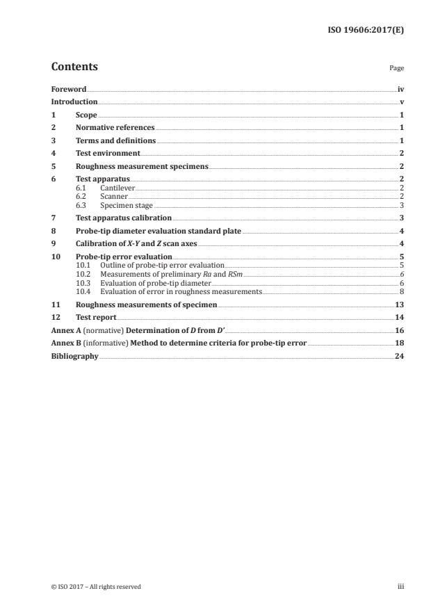
Contents Page
Foreword .iv
Introduction .v
1 Scope . 1
2 Normative references . 1
3 Terms and definitions . 1
4 Test environment . 2
5 Roughness measurement specimens . 2
6 Test apparatus . 2
6.1 Cantilever . 2
6.2 Scanner . 2
6.3 Specimen stage . 3
7 Test apparatus calibration . 3
8 Probe-tip diameter evaluation standard plate . 4
9 Calibration of X-Y and Z scan axes . 4
10 Probe-tip error evaluation . 5
10.1 Outline of probe-tip error evaluation . 5
10.2 Measurements of preliminary Ra and RSm .6
10.3 Evaluation of probe-tip diameter . 6
10.4 Evaluation of error in roughness measurements . 8
11 Roughness measurements of specimen .13
12 Test report .14
Annex A (normative) Determination of D from D’ .16
Annex B (informative) Method to determine criteria for probe-tip error .18
Bibliography .24
Foreword
ISO (the International Organization for Standardization) is a worldwide federation of national standards
bodies (ISO member bodies). The work of preparing International Standards is normally carried out
through ISO technical committees. Each member body interested in a subject for which a technical
committee has been established has the right to be represented on that committee. International
organizations, governmental and non-governmental, in liaison with ISO, also take part in the work.
ISO collaborates closely with the International Electrotechnical Commission (IEC) on all matters of
electrotechnical standardization.
The procedures used to develop this document and those intended for its further maintenance are
described in the ISO/IEC Directives, Part 1. In particular the different approval criteria needed for the
different types of ISO documents should be noted. This document was drafted in accordance with the
editorial rules of the ISO/IEC Directives, Part 2 (see www .iso .org/ directives).
Attention is drawn to the possibility that some of the elements of this document may be the subject of
patent rights. ISO shall not be held responsible for identifying any or all such patent rights. Details of
any patent rights identified during the development of the document will be in the Introduction and/or
on the ISO list of patent declarations received (see www .iso .org/ patents).
Any trade name used in this document is information given for the convenience of users and does not
constitute an endorsement.
For an explanation on the meaning of ISO specific terms and expressions related to conformity assessment,
as well as information about ISO’s adherence to the World Trade Organization (WTO) principles in the
Technical Barriers to Trade (TBT) see the following URL: www . i so .org/ iso/ foreword .html.
This document was prepared by Technical Committee ISO/TC 206, Fine ceramics.
iv © ISO 2017 – All rights reserved
Introduction
Surface roughness measurements of fine ceramic thin films in nanometer scale by atomic force
microscopy have become one of the techniques widely applied to quality control and assurance in
industries.
One of the problems most frequently occurring in roughness measurements by atomic force microscopy
resulting from its scale dependency is the deviation of roughness due to the wear of the probe tip or
the deviation in the curvature of commercially available probe tips. This problem makes it difficult to
obtain a reliable and reproducible result of the roughness measurement. Therefore, it is highly desirable
to standardize a method to evaluate probe tip diameter or curvature radius.
This document covers the evaluation of probe-tip diameter and provides a method to judge the
adequateness of a probe tip for use in day-to-day roughness measurements of fine ceramic thin films
with a certain arithmetical mean roughness in the range needing the use of atomic force microscopy in
production lines or quality assurance processes.
It should be noted that because surface roughness is a scale-dependent metrology parameter, it is
unavoidable that the probe-tip evaluation process contains some contradictory procedures, namely the
adequateness of the probe tip for a roughness measurement depends on unmeasurable true roughness
in a scale of interest.
In this document, the parameters based on roughness profiles are used. The roughness profile is
obtained by using a low-pass filter according to ISO 16610-21. The process to obtain the sampling
length, which is identical to cut-off wavelength, is given in ISO 4288. Some different sampling lengths to
process a primary profile can be applied to obtain appropriate values of arithmetic mean deviation of a
roughness profile, if necessary.
INTERNATIONAL STANDARD ISO 19606:2017(E)
Fine ceramics (advanced ceramics, advanced technical
ceramics) — Test method for surface roughness of fine
ceramic films by atomic force microscopy
1 Scope
This document describes a method to evaluate the adequateness of a probe tip for fine-ceramic thin-film
surface roughness measurements by atomic force microscopy, of surfaces with an arithmetical mean
roughness, Ra, in the range of about 1 nm to 30 nm and a mean width of roughness profile elements,
RSm, in the range of about 0,04 μm to 2,5 μm.
2 Normative references
The following documents are referred to in the text in such a way that some or all of their content
constitutes requirements of this document. For dated references, only the edition cited applies. For
undated references, the latest edition of the referenced document (including any amendments) applies.
ISO 4287, Geometrical Product Specifications (GPS) — Surface texture: Profile method — Terms, definitions
and surface texture parameters
ISO 4288, Geometrical Product Specifications (GPS) — Surface texture: Profile method — Rules and
procedures for the assessment of surface texture
ISO 11039, Surface chemical analysis — Scanning-probe microscopy — Measurement of drift rate
ISO 11952, Surface chemical analysis — Scanning-probe microscopy — Determination of geometric
quantities using SPM: Calibration of measuring systems
ISO 18115-2, Surface chemical analysis — Vocabulary — Part 2: Terms used in scanning-probe microscopy
ISO 25178-2, Geometrical product specifications (GPS) — Surface texture: Areal — Part 2: Terms, definitions
and surface texture parameters
3 Terms and definitions
For the purposes of this document, the terms and definitions given in ISO 4287, ISO 4288, ISO 18115-2,
ISO 11039, ISO 11952 and ISO 25178-2 and the following apply.
ISO and IEC maintain terminological databases for use in standardization at the following addresses:
— IEC Electropedia: available at http:// www .electropedia .org/
— ISO Online browsing platform: available at http:// www .iso .org/ obp
3.1
evaluation length
ln(X), ln(Y)
length of surface profile in the X or Y direction
3.2
probe-tip diameter evaluation standard plate
plate on which needle-shaped spikes are formed
Note 1 to entry: The plate is used to evaluate the probe-tip diameter (3.3).
3.3
probe-tip diameter
D
diameter of a probe tip at a distance of 10 nm from the tip end
4 Test environment
Testing shall be carried out only where temperature change, sound noise and mechanical vibration
of the floor or walls are small enough to perform the measurements. The following installation
environment is recommended:
a) temperature: 18 °C to 25 °C;
b) humidity: 70 % or less;
c) noise level: 60 dB or less;
−3 2
d) mechanical vibration of the floor or the wall: 1 × 10 m/s (<100 Hz) or less.
5 Roughness measurement specimens
Specimens for roughness measurements are ceramic thin films on a substrate. Any kinds of substrate
material can be used, such as metal, glass, polymer, etc. The specimen shall be no larger than the
specimen stage of the instrument being used.
6 Test apparatus
6.1 Cantilever
The cantilever shall be exclusively dedicated for a dynamic mode and commercially available. The
resonant frequency should be higher than 100 kHz.
6.2 Scanner
The scanner shall be capable of scanning cantilever or specimen stage by shifting the XYZ position. The
scanning area should be larger than 10 μm × 10 μm in the XY plane.
Figure 1 shows an example of a measurement system having a specimen stage scan mechanism.
Position in the Z direction is controlled using a Z-position control circuit that keeps a constant
separation between the probe and the specimen surface. For this purpose, a light beam from a laser
diode illuminates the cantilever and the reflected beam position is monitored by a light detector.
Surface profile is measured by scanning the specimen stage in the XY plane.
2 © ISO 2017 – All rights reserved
Key
1 laser diode 6 specimen stage
2 light detector 7 X, Y and Z scanner
3 cantilever 8 Z-position control circuit
4 probe tip 9 X-Y scan circuit
5 specimen
Figure 1 — Schematic of AFM system
6.3 Specimen stage
The specimen stage shall be capable of supporting a specimen horizontally. The test area of the
specimen should be in the centre of the specimen stage. Scanning should be performed near the centre
of the X, Y and Z axes of the scanner used.
7 Test apparatus calibration
This document only describes a method to evaluate the adequateness of a probe tip for fine-ceramic
thin-film surface roughness measurements by atomic force microscopy. If the apparatus needs to
be calibrated, refer to standards describing calibration criteria and methods for a scanning probe
microscope; see ISO 4288, ISO 11039 and ISO 11775.
8 Probe-tip diameter evaluation standard plate
A standard for probe-tip diameter evaluation is a plate on which a number of needle-shaped spikes,
arranged in a square matrix, are formed. The needle-shaped spikes are typically as follows:
— tip curvature radius: 10 nm;
— tip aperture angle: 20° or 50°;
— tip height: 300 nm to 600 nm;
— distance between any two nearest neighbour tips: 2,12 μm;
— plate size: 5 mm × 5 mm.
9 Calibration of X-Y and Z scan axes
The calibration of the X-Y scanner and Z scanner should be carried out by measuring the X, Y and Z
profile of a certified calibration standard. The standard should have a grating with a certain pitch and a
step with a certain height.
The standard sample is a specimen with calibrated height and pitch, which are certified and traceable
with uncertainty data attached. It is recommended that the grating pitch is less than 2 μm and that the
step height is less than 20 nm.
The calibration standard should be stored in a clean and dry box and be handled with care.
The calibration shall be carried out in the following sequence using the dynamic mode.
a) Mount the calibration standard in such a way that the grating is oriented to the X-Y axes of the
scanner and that its plane lies nearly parallel to the X-Y plane of the scanner.
b) Set the number of picture elements at 512 × 512 or 256 × 256.
c) Scan an area of about 10 μm square of the calibration standard and store the surface profile data.
An example is shown in Figure 2 a).
d) From the surface profile data, draw a surface profile along the X direction at a selected Y position
where the surface profile contains several steps on the calibration standard and level off the one-
dimensional profile along the X direction. An example is shown in Figure 2 b).
e) Measure profile peak height at the centre of top and bottom sections of the profile. Calculate mean
height for at least five successive profile elements in the profile along the X direction.
f) Measure a pitch along the X direction by measuring the distance between the mid-points of two
successive rising or falling parts of the profile.
g) From the surface profile data, draw a surface profile along the Y direction at a selected X position
where the surface profile contains several steps and level off the one-dimensional profile along the
Y direction.
h) Measure profile peak heights at the centre of top and bottom sections of the profile. Calculate mean
height for at least five successive profile elements in the profile along the Y direction.
i) Measure a pitch along the Y direction by measuring the distance between the mid-points of two
successive rising or falling parts of the profile.
j) If an X- or Y-pitch measured is out of the range of uncertainty needed for roughness measurements,
correct X or Y values by obtaining an X- or Y-axis calibration factor.
k) If the mean height obtained is out of the range of uncertainty needed for
...


Questions, Comments and Discussion
Ask us and Technical Secretary will try to provide an answer. You can facilitate discussion about the standard in here.
Loading comments...