IEC TS 62876-3-4:2025
(Main)Nanomanufacturing - Reliability assessment - Part 3-4: Linearity of output characteristics for metal contacted 2D semiconductor devices
Nanomanufacturing - Reliability assessment - Part 3-4: Linearity of output characteristics for metal contacted 2D semiconductor devices
IEC TS 62876-3-4:2025, which is a Technical Specification, establishes a standardized guideline to assess
• reliability of metallic interfaces
of Ohmic-contacted field-effect transistors (FETs) using 2D nano-materials by quantifying
• linearity of current-voltage (I-V) output curves
for devices with various materials combinations of van der Waals (vdW) interfaces.
For metallic interfaces with 2D materials (eg. graphene, MoS2, MoTe2, WS2, WSe2, etc) and metals (eg. Ti, Cr, Au, Pd, In, Sb, etc), the reliability of Ohmic contact is quantified.
For FETs consisting of 2D materials-based channels (eg. MoS2, MoTe2, WS2, WSe2, etc), the reliability of Ohmic contact when varying contacting metal, channel length, channel thickness, applied voltage, and surface treatment condition is quantified.
The reliability of the metallic contacts is quantified from the linearity of I-V characteristics measured over extended time periods.
General Information
- Status
- Published
- Publication Date
- 15-Dec-2025
- Technical Committee
- TC 113 - Nanotechnology for electrotechnical products and systems
- Drafting Committee
- WG 7 - TC 113/WG 7
- Current Stage
- PPUB - Publication issued
- Start Date
- 16-Dec-2025
- Completion Date
- 02-Jan-2026
Overview
IEC TS 62876-3-4:2025 is a Technical Specification in the IEC 62876 nanomanufacturing series that defines a standardized method to assess the reliability of metallic contacts in field‑effect transistors (FETs) built from 2D semiconductor materials. The document quantifies reliability by measuring and analysing the linearity of current–voltage (I–V) output characteristics for metal‑contacted 2D devices (e.g., MoS2, WSe2, WS2, MoTe2, graphene) with a range of metals (e.g., Ti, Cr, Au, Pd, In, Sb). Measurements are required over extended time periods to capture contact stability and degradation.
Key topics and technical requirements
- Scope and definitions: Terms for sample geometry, contacts (bottom, edge), and test conditions specific to 2D FETs and van der Waals (vdW) interfaces.
- Sample preparation: Recommended device structures, fabrication approaches and surface treatments (e.g., methods used to induce ohmic-like transport are illustrated in informative annexes).
- Measurement procedure:
- Required measurement equipment and calibration steps.
- Protocol for collecting output I–V curves (drain current vs drain voltage at varying gate voltages).
- Consideration of channel length, channel thickness, applied voltages and contact type.
- Data analysis and interpretation:
- Quantification of I–V linearity to distinguish Ohmic-like vs Schottky (non‑Ohmic) behaviour.
- Guidance on deriving contact reliability metrics from I–V linearity and time‑dependent datasets.
- Figures and derivative-based methods to identify current saturation and contact-limited conduction.
- Informative worked examples: Annexes present case studies (bottom‑contacted WSe2, edge‑contacted MoS2, WS2 with current saturation) illustrating reporting and analysis.
- Supporting tables and figures: e.g., allowed channel lengths for given contact‑resistance limits and schematic I–V examples.
Applications and users
This Technical Specification is practical for:
- Semiconductor researchers and device engineers developing 2D-material FETs.
- Materials scientists and process engineers evaluating metal–2D interfaces, contact metallurgy, and surface treatments.
- Reliability engineers and test labs establishing standardized I–V testing and long‑term contact stability protocols.
- Foundries and nanomanufacturing developers integrating 2D devices into electronic subsystems.
Use cases include validating Ohmic contact formation, comparing contacting metals and surface treatments, optimizing channel geometry for low contact resistance, and producing reproducible reliability data for device qualification.
Related standards
- Part of the IEC 62876 series: other parts address broader nanomanufacturing reliability topics (refer to IEC catalogue for related parts).
- Referenced measurement and calibration standards are listed in the normative references of the TS.
Keywords: IEC TS 62876-3-4:2025, nanomanufacturing, reliability assessment, 2D semiconductor devices, I–V linearity, Ohmic contact, van der Waals interface, contact resistance, FET measurement.
Frequently Asked Questions
IEC TS 62876-3-4:2025 is a technical specification published by the International Electrotechnical Commission (IEC). Its full title is "Nanomanufacturing - Reliability assessment - Part 3-4: Linearity of output characteristics for metal contacted 2D semiconductor devices". This standard covers: IEC TS 62876-3-4:2025, which is a Technical Specification, establishes a standardized guideline to assess • reliability of metallic interfaces of Ohmic-contacted field-effect transistors (FETs) using 2D nano-materials by quantifying • linearity of current-voltage (I-V) output curves for devices with various materials combinations of van der Waals (vdW) interfaces. For metallic interfaces with 2D materials (eg. graphene, MoS2, MoTe2, WS2, WSe2, etc) and metals (eg. Ti, Cr, Au, Pd, In, Sb, etc), the reliability of Ohmic contact is quantified. For FETs consisting of 2D materials-based channels (eg. MoS2, MoTe2, WS2, WSe2, etc), the reliability of Ohmic contact when varying contacting metal, channel length, channel thickness, applied voltage, and surface treatment condition is quantified. The reliability of the metallic contacts is quantified from the linearity of I-V characteristics measured over extended time periods.
IEC TS 62876-3-4:2025, which is a Technical Specification, establishes a standardized guideline to assess • reliability of metallic interfaces of Ohmic-contacted field-effect transistors (FETs) using 2D nano-materials by quantifying • linearity of current-voltage (I-V) output curves for devices with various materials combinations of van der Waals (vdW) interfaces. For metallic interfaces with 2D materials (eg. graphene, MoS2, MoTe2, WS2, WSe2, etc) and metals (eg. Ti, Cr, Au, Pd, In, Sb, etc), the reliability of Ohmic contact is quantified. For FETs consisting of 2D materials-based channels (eg. MoS2, MoTe2, WS2, WSe2, etc), the reliability of Ohmic contact when varying contacting metal, channel length, channel thickness, applied voltage, and surface treatment condition is quantified. The reliability of the metallic contacts is quantified from the linearity of I-V characteristics measured over extended time periods.
IEC TS 62876-3-4:2025 is classified under the following ICS (International Classification for Standards) categories: 07.120 - Nanotechnologies. The ICS classification helps identify the subject area and facilitates finding related standards.
IEC TS 62876-3-4:2025 is available in PDF format for immediate download after purchase. The document can be added to your cart and obtained through the secure checkout process. Digital delivery ensures instant access to the complete standard document.
Standards Content (Sample)
IEC TS 62876-3-4 ®
Edition 1.0 2025-12
TECHNICAL
SPECIFICATION
Nanomanufacturing - Reliability assessment -
Part 3-4: Linearity of output characteristics for metal contacted 2D
semiconductor devices
ICS 07.120 ISBN 978-2-8327-0928-3
All rights reserved. Unless otherwise specified, no part of this publication may be reproduced or utilized in any form or
by any means, electronic or mechanical, including photocopying and microfilm, without permission in writing from either
IEC or IEC's member National Committee in the country of the requester. If you have any questions about IEC copyright
or have an enquiry about obtaining additional rights to this publication, please contact the address below or your local
IEC member National Committee for further information.
IEC Secretariat Tel.: +41 22 919 02 11
3, rue de Varembé info@iec.ch
CH-1211 Geneva 20 www.iec.ch
Switzerland
About the IEC
The International Electrotechnical Commission (IEC) is the leading global organization that prepares and publishes
International Standards for all electrical, electronic and related technologies.
About IEC publications
The technical content of IEC publications is kept under constant review by the IEC. Please make sure that you have the
latest edition, a corrigendum or an amendment might have been published.
IEC publications search - IEC Products & Services Portal - products.iec.ch
webstore.iec.ch/advsearchform Discover our powerful search engine and read freely all the
The advanced search enables to find IEC publications by a publications previews, graphical symbols and the glossary.
variety of criteria (reference number, text, technical With a subscription you will always have access to up to date
committee, …). It also gives information on projects, content tailored to your needs.
replaced and withdrawn publications.
Electropedia - www.electropedia.org
The world's leading online dictionary on electrotechnology,
IEC Just Published - webstore.iec.ch/justpublished
Stay up to date on all new IEC publications. Just Published containing more than 22 500 terminological entries in English
details all new publications released. Available online and and French, with equivalent terms in 25 additional languages.
once a month by email. Also known as the International Electrotechnical Vocabulary
(IEV) online.
IEC Customer Service Centre - webstore.iec.ch/csc
If you wish to give us your feedback on this publication or
need further assistance, please contact the Customer
Service Centre: sales@iec.ch.
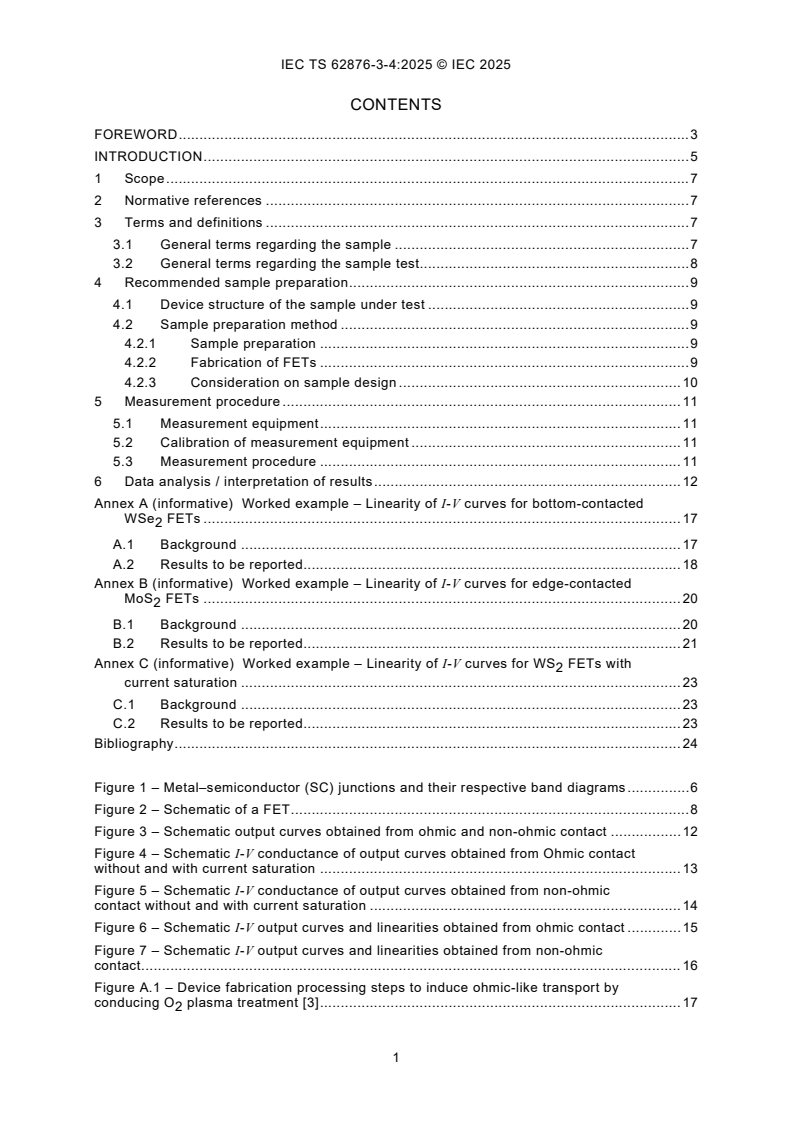
CONTENTS
FOREWORD . 3
INTRODUCTION . 5
1 Scope . 7
2 Normative references . 7
3 Terms and definitions . 7
3.1 General terms regarding the sample . 7
3.2 General terms regarding the sample test. 8
4 Recommended sample preparation . 9
4.1 Device structure of the sample under test . 9
4.2 Sample preparation method . 9
4.2.1 Sample preparation . 9
4.2.2 Fabrication of FETs . 9
4.2.3 Consideration on sample design . 10
5 Measurement procedure . 11
5.1 Measurement equipment . 11
5.2 Calibration of measurement equipment . 11
5.3 Measurement procedure . 11
6 Data analysis / interpretation of results . 12
Annex A (informative) Worked example – Linearity of I-V curves for bottom-contacted
WSe FETs . 17
A.1 Background . 17
A.2 Results to be reported. 18
Annex B (informative) Worked example – Linearity of I-V curves for edge-contacted
MoS FETs . 20
B.1 Background . 20
B.2 Results to be reported. 21
Annex C (informative) Worked example – Linearity of I-V curves for WS FETs with
current saturation . 23
C.1 Background . 23
C.2 Results to be reported. 23
Bibliography . 24
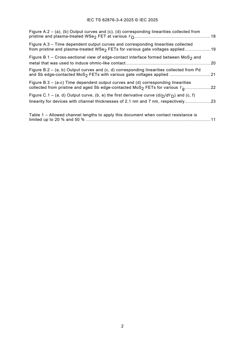
Figure 1 – Metal–semiconductor (SC) junctions and their respective band diagrams . 6
Figure 2 – Schematic of a FET . 8
Figure 3 – Schematic output curves obtained from ohmic and non-ohmic contact . 12
Figure 4 – Schematic I-V conductance of output curves obtained from Ohmic contact
without and with current saturation . 13
Figure 5 – Schematic I-V conductance of output curves obtained from non-ohmic
contact without and with current saturation . 14
Figure 6 – Schematic I-V output curves and linearities obtained from ohmic contact . 15
Figure 7 – Schematic I-V output curves and linearities obtained from non-ohmic
contact . 16
Figure A.1 – Device fabrication processing steps to induce ohmic-like transport by
conducing O plasma treatment [3] . 17
Figure A.2 – (a), (b) Output curves and (c), (d) corresponding linearities collected from
pristine and plasma-treated WSe FET at various V . 18
2 G
Figure A.3 – Time dependent output curves and corresponding linearities collected
from pristine and plasma-treated WSe FETs for various gate voltages applied . 19
Figure B.1 – Cross-sectional view of edge-contact interface formed between MoS and
metal that was used to induce ohmic-like contact . 20
Figure B.2 – (a, b) Output curves and (c, d) corresponding linearities collected from Pd
and Sb edge-contacted MoS FETs with various gate voltages applied . 21
Figure B.3 – (a-c) Time dependent output curves and (d) corresponding linearities
collected from pristine and aged Sb edge-contacted MoS FETs for various V . 22
2 g
Figure C.1 – (a, d) Output curve, (b, e) the first derivative curve (dI /dV ) and (c, f)
D D
linearity for devices with channel thicknesses of 2,1 nm and 7 nm, respectively . 23
Table 1 – Allowed channel lengths to apply this document when contact resistance is
limited up to 20 % and 50 % . 11
INTERNATIONAL ELECTROTECHNICAL COMMISSION
____________
Nanomanufacturing - Reliability assessment -
Part 3-4: Linearity of output characteristics for metal
contacted 2D semiconductor devices
FOREWORD
1) The International Electrotechnical Commission (IEC) is a worldwide organization for standardization comprising
all national electrotechnical committees (IEC National Committees). The object of IEC is to promote international
co-operation on all questions concerning standardization in the electrical and electronic fields. To this end and
in addition to other activities, IEC publishes International Standards, Technical Specifications, Technical Reports,
Publicly Available Specifications (PAS) and Guides (hereafter referred to as “IEC Publication(s)”). Their
preparation is entrusted to technical committees; any IEC National Committee interested in the subject dealt with
may participate in this preparatory work. International, governmental and non-governmental organizations liaising
with the IEC also participate in this preparation. IEC collaborates closely with the International Organization for
Standardization (ISO) in accordance with conditions determined by agreement between the two organizations.
2) The formal decisions or agreements of IEC on technical matters express, as nearly as possible, an international
consensus of opinion on the relevant subjects since each technical committee has representation from all
interested IEC National Committees.
3) IEC Publications have the form of recommendations for international use and are accepted by IEC National
Committees in that sense. While all reasonable efforts are made to ensure that the technical content of IEC
Publications is accurate, IEC cannot be held responsible for the way in which they are used or for any
misinterpretation by any end user.
4) In order to promote international uniformity, IEC National Committees undertake to apply IEC Publications
transparently to the maximum extent possible in their national and regional publications. Any divergence between
any IEC Publication and the corresponding national or regional publication shall be clearly indicated in the latter.
5) IEC itself does not provide any attestation of conformity. Independent certification bodies provide conformity
assessment services and, in some areas, access to IEC marks of conformity. IEC is not responsible for any
services carried out by independent certification bodies.
6) All users should ensure that they have the latest edition of this publication.
7) No liability shall attach to IEC or its directors, employees, servants or agents including individual experts and
members of its technical committees and IEC National Committees for any personal injury, property damage or
other damage of any nature whatsoever, whether direct or indirect, or for costs (including legal fees) and
expenses arising out of the publication, use of, or reliance upon, this IEC Publication or any other IEC
Publications.
8) Attention is drawn to the Normative references cited in this publication. Use of the referenced publications is
indispensable for the correct application of this publication.
9) IEC draws attention to the possibility that the implementation of this document may involve the use of (a)
patent(s). IEC takes no position concerning the evidence, validity or applicability of any claimed patent rights in
respect thereof. As of the date of publication of this document, IEC had not received notice of (a) patent(s), which
may be required to implement this document. However, implementers are cautioned that this may not represent
the latest information, which may be obtained from the patent database available at https://patents.iec.ch. IEC
shall not be held responsible for identifying any or all such patent rights.
IEC TS 62876-3-4 has been prepared by IEC technical committee 113: Nanotechnology for
electrotechnical products and systems. It is a Technical Specification.
The text of this Technical Specification is based on the following documents:
Draft Report on voting
113/920/DTS 113/938/RVDTS
Full information on the voting for its approval can be found in the report on voting indicated in
the above table.
The language used for the development of this Technical Specification is English.
This document was drafted in accordance with ISO/IEC Directives, Part 2, and developed in
accordance with ISO/IEC Directives, Part 1 and ISO/IEC Directives, IEC Supplement, available
at www.iec.ch/members_experts/refdocs. The main document types developed by IEC are
described in greater detail at www.iec.ch/publications.
A list of all parts in the IEC 62876 series, published under the general title Nanomanufacturing -
Reliability assessment, can be found on the IEC website.
The committee has decided that the contents of this document will remain unchanged until the
stability date indicated on the IEC website under webstore.iec.ch in the data related to the
specific document. At this date, the document will be
– reconfirmed,
– withdrawn, or
– revised.
INTRODUCTION
– Atomically thin two dimensional (2D) nano-materials are expected to be used for future
electrical sub-systems or electronic device applications.
– I-V measurements are the fundamental electrical characterization technique for assessing
reliability of field-effect transistors (FETs) as well as semiconductor device performance.
– The performance of the FET is mainly characterized by measuring the output (drain current
as a function of drain voltage at different gate voltages) and transfer (drain current as a
function of gate voltage at different drain voltages) characteristics.
– If metallic electrical contacts have negligible effects on electronic transport, output
characteristics show a linear behaviour according to the following formula:
μWC
n ox
I V−VV , where I is the drain current, μ is the electron mobility, W is the
( ) d
d g th d n
L
transport channel width, C is the gate oxide capacitance, V is the gate voltage, V is the
ox g th
threshold voltage, and V is the drain voltage, which can indicate ohmic contact. In contrast,
d
when metallic contact gives rise to high resistance to electronic transport, output
characteristics do not show the linear behaviour, following the formula:
μWC
n ox
I VV− V−×I 2R [1] where R is the contact resistance, which is
( )
( )
D g th dd C c
L
interpreted as Schottky contact which can bring about a reliability issue of ohmic-contact
semiconductor transistor operation.
– Current transport at the metallic contact of 2D semiconductor material-based FETs mainly
consists of two distinct components: thermal emission where charge injection occurs over
the energy barrier and tunnelling (field emission) where the charge injection occurs through
the barrier formed at the metal-semiconductor interface.
– Current transport at the metallic contact of 2D material-based FETs can be limited due to
the van der Waals (vdW) gap that forms at the metal-2D semiconductor interface, creating
a high contact resistance and suppressing current transport of the 2D FETs. However, being
different from 2D material-based FETs, conventional FETs have good ohmic contact and
usually have not had reliability issues in metallic contacts. But 2D materials involving vdW
gap can give rise to uncontrollable Schottky contact leading to a serious reliability issue of
metallic contact. See Figure 1.
– In addition, the lack of efficient doping techniques for 2D materials at the metal-
semiconductor junction, also contributes to the high contact resistance and suppressed
current transport, in contrast to 3D bulk semiconductors such as silicon. See Figure 1 for
comparison.
– The issues arising from the vdW gap at the 2D material-metal interface and thus the resulted
high contact resistance pose challenges to the reliability of metallic electrical contacts of 2D
FETs. Therefore, we propose a standard method to quantify the reliability of the metallic
electrical contacts by analyzing current-voltage (I-V) characteristics of 2D FETs.
=
=
a) Typical metal/bulk SC interface b) Au-MoS interface with vdW
Key
E Fermi level of metal
F
E conduction band of 2D SC
c
E valence band of 2D SC
v
TB tunnel barrier height
SB Schottky barrier height
A, B, B’ and C Different regions in the current path from the metal to the SC.
Blue arrows from top to bottom: Thermionic emission, thermionic field emission, and field emission (tunnelling).
Figure 1 – Metal–semiconductor (SC) junctions and their respective band diagrams
– Therefore, it is important to obtain accurate current-voltage (I-V) characteristics and to
assess linearity of the I-V output curves, so that reliable 2D FET device operation can be
ensured. The reliability of the devices also needs to be evaluated over an extended time
period.
NOTE Both capital and small letters in subscripts of device parameters are used with no differences each other,
dependent on users (typically device engineers): e.g. I is the same as I , V is the same as V , and V is the same
D d D d G
as V .
g
1 Scope
This part of IEC 62876 establishes a standardized guideline to assess
– reliability of metallic interfaces
of ohmic-contacted field-effect transistors (FETs) using 2D nano-materials by quantifying
– linearity of current-voltage (I-V) output curves
for devices with various materials combinations of van der Waals (vdW) interfaces.
For metallic interfaces with 2D materials (eg. graphene, MoS , MoTe , WS , WSe , etc) and
2 2 2 2
metals (eg. Ti, Cr, Au, Pd, In, Sb, etc), the reliability of ohmic contact is quantified.
For FETs consisting of 2D materials-based channels (eg. MoS , MoTe , WS , WSe , etc), the
2 2 2 2
reliability of ohmic contact when varying contacting metal, channel length, channel thickness,
applied voltage, and surface treatment condition is quantified.
The reliability of the metallic contacts is quantified from the linearity of I-V characteristics
measured over extended time periods.
2 Normative references
The following documents are referred to in the text in such a way that some or all of their content
constitutes requirements of this document. For dated references, only the edition cited applies.
For undated references, the latest edition of the referenced document (including any
amendments) applies.
IEC TS 62607-6-5, Nanomanufacturing - Key control characteristics - Part 6-5: Graphene-
based materials - Contact and sheet resistance: transmission line measurement
3 Terms and definitions
For the purposes of this document, the following terms and definitions apply.
ISO and IEC maintain terminology databases for use in standardization at the following
addresses:
– IEC Electropedia: available at https://www.electropedia.org/
– ISO Online browsing platform: available at https://www.iso.org/obp
3.1 General terms regarding the sample
3.1.1
two-dimensional material
material which has its thickness constrained within the nanoscale or smaller and consist of
between one and several layers
Note 1 to entry: These materials are thus termed two-dimensional (2D) materials as they have one dimension at
the nanoscale or smaller, with the other two dimensions generally at scales larger than the nanoscale.
EXAMPLE Graphene, monolayer and few layer versions of hexagonal boron nitride, molybdenum disulphi
...


Questions, Comments and Discussion
Ask us and Technical Secretary will try to provide an answer. You can facilitate discussion about the standard in here.
Loading comments...