EN 61188-5-1:2002
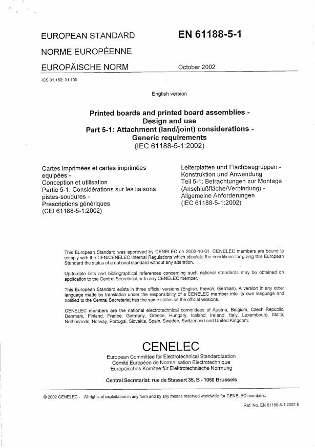
(Main)Printed boards and printed board assemblies - Design and use - Part 5-1: Attachment (land/joint) considerations - Generic requirements
Printed boards and printed board assemblies - Design and use - Part 5-1: Attachment (land/joint) considerations - Generic requirements
Provides information on land pattern geometries used for the surface attachment of electronic components. The intent of the information presented herein is to provide the appropriate size, shape and tolerance of surface-mount land patterns to insure sufficient area for the appropriate solder fillet, and also to allow for inspection, testing, and rework of those solder joints.
Leiterplatten und Flachbaugruppen - Konstruktion und Anwendung - Teil 5-1: Betrachtungen zur Montage (Anschlußfläche/Verbindung) - Allgemeine Anforderungen
Cartes imprimées et cartes imprimées équipées - Conception et utilisation - Partie 5-1: Considérations sur les liaisons pistes-soudures - Prescriptions génériques
Donne des informations sur les géométries des zones de report utilisées pour la fixation en surface des composants électroniques. Son intention est d'indiquer la taille, la forme et la tolérance appropriées des zones de report de montage en surface afin de garantir une surface suffisante pour le filet de soudure et de permettre également les inspections, les essais et les reprises de ces soudures.
Printed boards and printed board assemblies - Design and use - Part 5-1: Attachment (land/joint) considerations - Generic requirements
General Information
Relations
Standards Content (Sample)
SLOVENSKI SIST EN 61188-5-1:2003
STANDARD
april 2003
Printed boards and printed board assemblies - Design and use - Part 5-1:
Attachment (land/joint) considerations - Generic requirements
ICS 31.180 Referenčna številka
© Standard je založil in izdal Slovenski inštitut za standardizacijo. Razmnoževanje ali kopiranje celote ali delov tega dokumenta ni dovoljeno
NORME CEI
INTERNATIONALE IEC
61188-5-1
INTERNATIONAL
Première édition
STANDARD
First edition
2002-07
Cartes imprimées et cartes imprimées équipées –
Conception et utilisation –
Partie 5-1:
Considérations sur les liaisons pistes-soudures –
Prescriptions génériques
Printed boards and printed board assemblies –
Design and use –
Part 5-1:
Attachment (land/joint) considerations –
Generic requirements
© IEC 2002 Droits de reproduction réservés ⎯ Copyright - all rights reserved
Aucune partie de cette publication ne peut être reproduite ni No part of this publication may be reproduced or utilized in any
utilisée sous quelque forme que ce soit et par aucun procédé, form or by any means, electronic or mechanical, including
électronique ou mécanique, y compris la photocopie et les photocopying and microfilm, without permission in writing from
microfilms, sans l'accord écrit de l'éditeur. the publisher.
International Electrotechnical Commission, 3, rue de Varembé, PO Box 131, CH-1211 Geneva 20, Switzerland
Telephone: +41 22 919 02 11 Telefax: +41 22 919 03 00 E-mail: inmail@iec.ch Web: www.iec.ch
CODE PRIX
XB
Commission Electrotechnique Internationale PRICE CODE
International Electrotechnical Commission
ɆɟɠɞɭɧɚɪɨɞɧɚɹɗɥɟɤɬɪɨɬɟɯɧɢɱɟɫɤɚɹɄɨɦɢɫɫɢɹ
Pour prix, voir catalogue en vigueur
For price, see current catalogue
61188-5-1 © IEC:2002 – 3 –
CONTENTS
FOREWORD .11
1 Scope and object .15
2 Normative references.15
3 Terms and definitions.17
4 Design requirements .29
4.1 General .29
4.1.1 Classification .31
4.1.2 Land pattern determination.31
4.2 Dimensioning systems .33
4.2.1 Component tolerancing .35
4.2.2 Land tolerancing .43
4.2.3 Fabrication allowances .43
4.2.4 Assembly tolerancing .43
4.2.5 Dimension and tolerance analysis.45
4.3 Design producibility.61
4.3.1 SMT land pattern.63
4.3.2 Standard component selection .63
4.3.3 Circuit substrate development .63
4.3.4 Assembly considerations .63
4.3.5 Provision for automated test.63
4.3.6 Documentation for SMT.63
4.4 Environmental constraint.63
4.4.1 Moisture sensitive components.63
4.4.2 End-use environment considerations .65
4.5 Design rules.67
4.5.1 Component spacing .67
4.5.2 Single- and double-sided board assembly.71
4.5.3 Solder paste stencil.71
4.5.4 Component stand-off height for cleaning .71
4.5.5 Fiducial marks.73
4.5.6 Conductors .79
4.5.7 Via guidelines .81
4.5.8 Standard fabrication allowances .85
4.5.9 Panelization .89
4.6 Outer layer finishes .95
4.6.1 Solder-mask finishes.95
4.6.2 Solder-mask clearances .95
4.6.3 Land-pattern finishes.97
5 Quality and reliability validation .97
5.1 Validation techniques .97
6 Testability .99
6.1 Five types of testing .99
6.1.1 Bare-board test .99
6.1.2 Assembled board test.101
61188-5-1 © IEC:2002 – 5 –
6.2 Nodal access .101
6.2.1 Test philosophy.101
6.2.2 Test strategy for bare boards .103
6.3 Full nodal access for assembled board.103
6.3.1 In-circuit test accommodation.105
6.3.2 Multi-probe testing .105
6.4 Limited nodal access .105
6.5 No nodal access .107
6.6 Clam-shell fixtures impact .107
6.7 Printed board test characteristics .107
6.7.1 Test land pattern spacing .107
6.7.2 Test land size and shape.107
6.7.3 Design for test parameters .109
7 Printed board structure types.111
7.1 General considerations .115
7.1.1 Categories .117
7.1.2 Thermal expansion mismatch.117
7.2 Organic base material .117
7.3 Non-organic base materials.117
7.4 Alternative PB structures.117
7.4.1 Supporting-plane PB structures .117
7.4.2 High-density PB technology.117
7.4.3 Discrete-wire interconnect .119
7.4.4 Constraining core structures.119
7.4.5 Porcelainized metal (metal core) structures .119
8 Assembly considerations for surface-mount technology (SMT).119
8.1 SMT assembly process sequence .119
8.2 Substrate preparation.121
8.2.1 Adhesive application .121
8.2.2 Conductive adhesive .123
8.2.3 Solder paste application .123
8.2.4 Solder preforms .123
8.3 Component placement .123
8.3.1 Component data transfer.123
8.4 Soldering processes.125
8.4.1 Wave soldering .125
8.4.2 Vapour-phase soldering .127
8.4.3 IR reflow .129
8.4.4 Hot air/gas convection.129
8.4.5 Laser reflow soldering .129
8.5 Cleaning .129
8.6 Repair/rework .131
8.6.1 Re-use of removed components .131
8.6.2 Heatsink effects .131
8.6.3 Dependence on printed board material type.133
8.6.4 Dependence on copper land and conductor layout .133
8.6.5 Selection of suitable rework equipment.133
8.6.6 Dependence on assembly structure and soldering processes.133
61188-5-1 © IEC:2002 – 7 –
Annex A (informative) Test patterns – Process evaluations .135
Annex B (informative) Abbreviations .141
Figure 1 – Profile tolerancing method.33
Figure 2 – Example of 3216 capacitor dimensioning for optimum solder fillet condition.37
Figure 3 – Profile dimensioning of gull-wing leaded SOIC.39
Figure 4 – Pitch for multiple leaded component.49
Figure 5 – Courtyard boundary area condition.59
Figure 6 – Component orientation for wave-solder applications .67
Figure 7 – Alignment of similar components.69
Figure 8 – Panel/local fiducials .73
Figure 9 – Local and global fiducials .75
Figure 10 – Fiducial locations on a printed board .75
Figure 11 – Fiducial clearance requirements.77
Figure 12 – Surface mounting geometries.79
Figure 13 – Conductor routing capability test pattern.81
Figure 14 – Land-pattern-to-via relationship .83
Figure 15 – Examples of via positioning concepts .83
Figure 16 – Conductor description .87
Figure 17 – Examples of modified landscapes .89
Figure 18 – Typical copper glass laminate panel .91
Figure 19 – Conductor clearance for V-groove scoring .91
Figure 20 – Breakaway (routed
...


Questions, Comments and Discussion
Ask us and Technical Secretary will try to provide an answer. You can facilitate discussion about the standard in here.