ASTM B667-97(2009)
(Practice)Standard Practice for Construction and Use of a Probe for Measuring Electrical Contact Resistance
Standard Practice for Construction and Use of a Probe for Measuring Electrical Contact Resistance
SIGNIFICANCE AND USE
Electrical contact resistance is an important characteristic of the contact in certain components, such as connectors, switches, slip rings, and relays. Ordinarily, contact resistance is required to be low and stable for proper functioning of many devices or apparatus in which the component is used. It is more convenient to determine contact resistance with a probe than to incorporate the contact material into an actual component for the purpose of measurement. However, if the probe contact material is different from that employed in the component, the results obtained may not be applicable to the device.
Information on contact resistance is useful in materials development, in failure analysis studies, in the manufacturing and quality control of contact devices, and in research.
Contact resistance is not a unique single-valued property of a material. It is affected by the mechanical conditions of the contact, the geometry and roughness of contacting surfaces, surface cleanliness, and contact history, as well as by the material properties of hardness and conductivity of both contacting members. An objective of this practice is to define and control many of the known variables in such a way that valid comparisons of the contact properties of materials can be made.
In some techniques for measuring contact resistance it is not possible to eliminate bulk resistance, that is, the resistance of the metal pieces comprising the contact and the resistance of the wires and connections used to introduce the test current into the samples. In these cases, the measurement is actually of an overall resistance, which is often confused with contact resistance.
SCOPE
1.1 This practice describes equipment and techniques for measuring electrical contact resistance with a probe and the presentation of results.
1.2 The values stated in SI units are to be regarded as standard. No other units of measurement are included in this standard.
1.3 This standard does not purport to address all of the safety concerns, if any, associated with its use. It is the responsibility of the user of this standard to become familiar with all hazards including those identified in the appropriate Material Safety Data Sheet (MSDS) for this product/material as provided by the manufacturer, to establish appropriate safety and health practices, and determine the applicability of regulatory limitations prior to use.
General Information
Relations
Buy Standard
Standards Content (Sample)
NOTICE: This standard has either been superseded and replaced by a new version or withdrawn.
Contact ASTM International (www.astm.org) for the latest information
Designation: B667 − 97 (Reapproved2009)
Standard Practice for
Construction and Use of a Probe for Measuring Electrical
Contact Resistance
This standard is issued under the fixed designation B667; the number immediately following the designation indicates the year of
original adoption or, in the case of revision, the year of last revision. A number in parentheses indicates the year of last reapproval. A
superscript epsilon (´) indicates an editorial change since the last revision or reapproval.
1. Scope they funnel through these tiny areas. If oxide films or other
insulating layers interfere with these metal-to-metal contacts,
1.1 This practice describes equipment and techniques for
the contact resistance will be higher than when such layers are
measuring electrical contact resistance with a probe and the
absent (see 4.4 for bulk resistance limitation).
presentation of results.
3.2.2 contact resistance probe, n—an apparatus for deter-
1.2 The values stated in SI units are to be regarded as
mining electrical contact resistance characteristics of a metal
standard. No other units of measurement are included in this
surface. Probe, in this instance, should be distinguished from
standard.
the classical tool whose function it is to touch or move an
1.3 This standard does not purport to address all of the
object.
safety concerns, if any, associated with its use. It is the
responsibility of the user of this standard to become familiar
4. Significance and Use
with all hazards including those identified in the appropriate
Material Safety Data Sheet (MSDS) for this product/material
4.1 Electrical contact resistance is an important characteris-
as provided by the manufacturer, to establish appropriate
tic of the contact in certain components, such as connectors,
safety and health practices, and determine the applicability of
switches,sliprings,andrelays.Ordinarily,contactresistanceis
regulatory limitations prior to use.
required to be low and stable for proper functioning of many
devicesorapparatusinwhichthecomponentisused.Itismore
2. Referenced Documents
convenient to determine contact resistance with a probe than to
2.1 ASTM Standards:
incorporate the contact material into an actual component for
B542 Terminology Relating to Electrical Contacts and Their
the purpose of measurement. However, if the probe contact
Use
material is different from that employed in the component, the
results obtained may not be applicable to the device.
3. Terminology
4.2 Information on contact resistance is useful in materials
3.1 Definitions—Many terms used in this practice are de-
development, in failure analysis studies, in the manufacturing
fined in Terminology B542.
and quality control of contact devices, and in research.
3.2 Definitions of Terms Specific to This Standard:
4.3 Contactresistanceisnotauniquesingle-valuedproperty
3.2.1 contact resistance, n—the resistance to current flow
of a material. It is affected by the mechanical conditions of the
between two touching bodies, consisting of constriction resis-
contact, the geometry and roughness of contacting surfaces,
tance and film resistance.
surface cleanliness, and contact history, as well as by the
3.2.1.1 Discussion—Constrictionresistanceoriginatesinthe
material properties of hardness and conductivity of both
fact that mating surfaces touch in most cases at only their high
contacting members. An objective of this practice is to define
spots, which are often called“ asperities” or, more commonly,
and control many of the known variables in such a way that
a-spots. The current flow lines are then forced to constrict as
valid comparisons of the contact properties of materials can be
made.
This practice is under the jurisdiction ofASTM Committee B02 on Nonferrous
Metals and Alloys and is the direct responsibility of Subcommittee B02.11 on
4.4 In some techniques for measuring contact resistance it is
Electrical Contact Test Methods.
not possible to eliminate bulk resistance, that is, the resistance
Current edition approved April 15, 2009. Published April 2009. Originally
ϵ1
of the metal pieces comprising the contact and the resistance of
approved in 1980. Last previous edition approved in 2003 as B667 – 97 (2003) .
DOI: 10.1520/B0667-97R09.
thewiresandconnectionsusedtointroducethetestcurrentinto
For referenced ASTM standards, visit the ASTM website, www.astm.org, or
the samples. In these cases, the measurement is actually of an
contact ASTM Customer Service at service@astm.org. For Annual Book of ASTM
overall resistance, which is often confused with contact resis-
Standards volume information, refer to the standard’s Document Summary page on
the ASTM website. tance.
Copyright © ASTM International, 100 Barr Harbor Drive, PO Box C700, West Conshohocken, PA 19428-2959. United States
B667 − 97 (2009)
5. General Description of a Probe large stresses at the tops of small asperities. Likewise, bounce
should be avoided when touching the probe to the specimen.
5.1 A probe generally includes the following:
Vibration may reveal itself as a noisy signal when contact
5.1.1 Fixtures for holding specimens of varied size and
resistance is continuously monitored electronically.
shape and for attaching electrical leads to them.
6.4.1 For sensitive surfaces, a preliminary run should be
5.1.2 A mechanism that applies a measurable load to the
made on as-received (uncleaned) test specimens of the same
specimen that can be increased, decreased, or held constant.
surface material as the samples to be measured. If the
5.1.3 A shock mounted table to prevent any indigenous
vibration-inducedfluctuationsaregreaterthan10 %,additional
vibrations from inadvertently altering the conditions at the
antivibrational measures should be taken.
contact interface.
6.4.2 Wipe should not be introduced when contact resis-
5.1.4 Areference surface (the probe) that is pressed against
tance versus load characteristics are being measured, since as
the specimen and which is normally made of a noble metal.
little as a few micrometers of lateral movement can drastically
Noble metals such as pure gold are used because they are
change the contact resistance of samples having films.
substantially free of oxide films and have the best likelihood of
obtaining reproducible results.
NOTE 1—Some variation of contact resistance with time under load has
5.1.5 A current source with current and voltage measuring
beenfoundtooccurformanymaterials. Itisthereforerecommendedthat,
for continuously monitored runs, the resistance at the final applied load
instrumentation for determining contact resistance. Ordinarily,
should also be recorded after a fixed dwell time, usually 10 to 30 s.
contact resistance is determined at dry circuit conditions to
avoid changes that may occur due to voltage breakdown or
6.5 The power supply shall be capable of delivering a
heating at the contact interface. pulse-free source under dry circuit conditions. To avoid errors
that may arise due to contact potentials and thermal EMF’s all
5.2 Additional electrical circuitry may be included to permit
d-c measurements should be taken with forward and reverse
related measurements to be obtained, such as the voltage
voltages and the results averaged. Measurements taken with
breakdown or the current versus voltage characteristics of
low frequency a-c sources automatically compensate for this
film-covered surfaces.
error.
5.3 Probes are also convenient for determining the depen-
dence of contact resistance on sliding or wipe when a slide is
7. Requirements of the Probe Contact
incorporated in the specimen holder. This permits the probe to
7.1 The probe is normally made with a pure gold surface,
be moved small measurable distances after loading.
although other noble metals can be used. The probe should be
smooth and have a large radius of curvature to minimize the
6. Design Aspects
possibility that it may damage the specimen surface. An
6.1 The probe is mounted on one end of a pivoted beam, a
exception to this latter recommendation are the wire probes
cantilever, or a coil spring. Force is applied by dead weight,
that are generally designed for low normal loads (6.3).
compression of the spring, bending of the cantilever, or
7.1.1 One early probe design that has seen much use is a
electromagnetically.
3.2-mm diameter solid gold rod having a hemispherical end.
6.2 Probe holders have been designed so that force may be
Such probes have been used extensively to loads of 10 N.They
applied to the contact and to an electronic load cell which is
can be made by machining gold rods to finish dimensions,
mounted between the probe contact and a micrometer spindle
followed by burnishing with a glass microscope slide or other
that can be advanced. An alternative design is to mount the
hard smooth surface, using care to maintain the radius of the
specimen on the load cell and to advance the probe directly
end.
with the micrometer spindle. Load and contact resistance are
7.1.2 Other common probe types are solid gold rivets
the usual parameters measured and recorded simultaneously.
coined to a spherical end, with a radius of curvature of 1.6 mm,
6.3 A probe can be made by mounting a U-shaped free- as well as balls or hemispheres of similar radius of curvature.
standing gold wire to the micrometer spindle (see Fig. 1(b)). Pure gold platings have also been used successfully on these
The load is measured after the probe is observed (preferably spherical surfaces.
electrically) to first touch the specimen from a preliminary 7.1.3 In special cases, materials other than noble metals and
calibration (with a load cell) of m
...
This document is not anASTM standard and is intended only to provide the user of anASTM standard an indication of what changes have been made to the previous version. Because
it may not be technically possible to adequately depict all changes accurately, ASTM recommends that users consult prior editions as appropriate. In all cases only the current version
of the standard as published by ASTM is to be considered the official document.
´1
Designation:B667–97(Reapproved2003) Designation:B667–97(Reapproved2009)
Standard Practice for
Construction and Use of a Probe for Measuring Electrical
Contact Resistance
This standard is issued under the fixed designation B 667; the number immediately following the designation indicates the year of
original adoption or, in the case of revision, the year of last revision. A number in parentheses indicates the year of last reapproval. A
superscript epsilon (´) indicates an editorial change since the last revision or reapproval.
´ NOTE—Keywords were added editorially in December 2003.
1. Scope
1.1 This practice describes equipment and techniques for measuring electrical contact resistance with a probe and the
presentation of results.
1.2The values stated in SI units are to be regarded as standard. The values given in parentheses are for information only.
1.2 The values stated in SI units are to be regarded as standard. No other units of measurement are included in this standard.
1.3 This standard does not purport to address all of the safety concerns, if any, associated with its use. It is the responsibility
of the user of this standard to become familiar with all hazards including those identified in the appropriate Material Safety Data
Sheet (MSDS) for this product/material as provided by the manufacturer, to establish appropriate safety and health practices, and
determine the applicability of regulatory limitations prior to use.
2. Referenced Documents
2.1 ASTM Standards:
B 542 Terminology Relating to Electrical Contacts and Their Use
3. Terminology
3.1 Definitions—Many terms used in this practice are defined in Terminology B 542.
3.2 Definitions of Terms Specific to This Standard:
3.2.1 contact resistancecontact resistance, n—the resistance to current flow between two touching bodies, consisting of
constriction resistance and film resistance.
3.2.1.1 Discussion—Constriction resistance originates in the fact that mating surfaces touch in most cases at only their high
spots, which are often called “ asperities” or, more commonly, a-spots. The current flow lines are then forced to constrict as they
funnel through these tiny areas. If oxide films or other insulating layers interfere with these metal-to-metal contacts, the contact
resistance will be higher than when such layers are absent (see 4.4 for bulk resistance limitation).
3.2.2 contact resistance probecontact resistance probe, n—an apparatus for determining electrical contact resistance charac-
teristics of a metal surface. Probe, in this instance, should be distinguished from the classical tool whose function it is to touch
or move an object.
4. Significance and Use
4.1 Electricalcontactresistanceisanimportantcharacteristicofthecontactincertaincomponents,suchasconnectors,switches,
slip rings, and relays. Ordinarily, contact resistance is required to be low and stable for proper functioning of many devices or
apparatus in which the component is used. It is more convenient to determine contact resistance with a probe than to incorporate
the contact material into an actual component for the purpose of measurement. However, if the probe contact material is different
from that employed in the component, the results obtained may not be applicable to the device.
4.2 Information on contact resistance is useful in materials development, in failure analysis studies, in the manufacturing and
quality control of contact devices, and in research.
4.3 Contact resistance is not a unique single-valued property of a material. It is affected by the mechanical conditions of the
contact, the geometry and roughness of contacting surfaces, surface cleanliness, and contact history, as well as by the material
This practice is under the jurisdiction ofASTM Committee B02 on Nonferrous Metals andAlloys and is the direct responsibility of Subcommittee B02.11 on Electrical
Contact Test Methods.
Current edition approved Dec. 9, 2003. Published December 2003. Originally approved in 1980. Last previous edition approved in 1997 as B667–97.
´1
Current edition approved April 15, 2009. Published April 2009. Originally approved in 1980. Last previous edition approved in 2003 as B 667 – 97 (2003) .
For referencedASTM standards, visit theASTM website, www.astm.org, or contactASTM Customer Service at service@astm.org. For Annual Book of ASTM Standards
volume information, refer to the standard’s Document Summary page on the ASTM website.
Copyright © ASTM International, 100 Barr Harbor Drive, PO Box C700, West Conshohocken, PA 19428-2959, United States.
B667–97 (2009)
properties of hardness and conductivity of both contacting members. An objective of this practice is to define and control many
of the known variables in such a way that valid comparisons of the contact properties of materials can be made.
4.4 In some techniques for measuring contact resistance it is not possible to eliminate bulk resistance, that is, the resistance of
the metal pieces comprising the contact and the resistance of the wires and connections used to introduce the test current into the
samples. In these cases, the measurement is actually of an overall resistance, which is often confused with contact resistance.
5. General Description of a Probe
5.1 A probe generally includes the following:
5.1.1 Fixtures for holding specimens of varied size and shape and for attaching electrical leads to them.
5.1.2 A mechanism that applies a measurable load to the specimen that can be increased, decreased, or held constant.
5.1.3 A shock mounted table to prevent any indigenous vibrations from inadvertently altering the conditions at the contact
interface.
5.1.4 Areference surface (the probe) that is pressed against the specimen and which is normally made of a noble metal. Noble
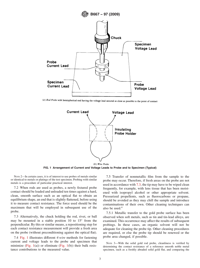
FIG. 1 Arrangement of Current and Voltage Leads to Probe and to Specimen (Typical)
metals such as pure gold are used because they are substantially free of oxide films and have the best likelihood of obtaining
reproducible results.
5.1.5 A current source with current and voltage measuring instrumentation for determining contact resistance. Ordinarily,
B667–97 (2009)
contact resistance is determined at dry circuit conditions to avoid changes that may occur due to voltage breakdown or heating
at the contact interface.
5.2 Additional electrical circuitry may be included to permit related measurements to be obtained, such as the voltage
breakdown or the current versus voltage characteristics of film-covered surfaces.
5.3 Probes are also convenient for determining the dependence of contact resistance on sliding or wipe when a slide is
incorporated in the specimen holder. This permits the probe to be moved small measurable distances after loading.
6. Design Aspects
6.1 The probe is mounted on one end of a pivoted beam, a cantilever, or a coil spring. Force is applied by dead weight,
compression of the spring, bending of the cantilever, or electromagnetically.
6.2 Probeholdershavebeendesignedsothatforcemaybeappliedtothecontactandtoanelectronicloadcellwhichismounted
between the probe contact and a micrometer spindle that can be advanced.An alternative design is to mount the specimen on the
load cell and to advance the probe directly with the micrometer spindle. Load and contact resistance are the usual parameters
measured and recorded simultaneously.
6.3 A probe can be made by mounting a U-shaped free-standing gold wire to the micrometer spindle (see Fig. 1(b)). The load
is measured after the probe is observed (preferably electrically) to first touch the specimen from a preliminary calibration (with
a load cell) of micrometer advance versus load. In some cases, where very small (to tens of milligrams) forces are used, it may
not be necessary to know the load precisely. In such cases, fine (for example, 50-µm diameter), straight, or U-shaped gold or
platinum wires can be used as the probe.
6.4 The apparatus must be isolated from vibration to avoid damaging the surface film that may exist at the interface to be
evaluated. The slightest movement can translate into extremely large stresses at the tops of small asperities. Likewise, bounce
should be avoided when touching the probe to the specimen. Vibration may reveal itself as a noisy signal when contact resistance
is continuously monitored electronically.
6.4.1 For sensitive surfaces, a preliminary run should be made on as-received (uncleaned) test specimens of the same surface
material as the samples to be measured. If the vibration-induced fluctuations are greater than 10 %, additional antivibrational
measures should be taken.
6.4.2 Wipe should not be introduced when contact resistance versus load characteristics are being measured, since as little as
a few micrometers of lateral movement can drastically change the contact resistance of samples having films.
NOTE 1—Some variation of contact resistance with time under load has been found to occur for many materials. It is therefore recommended that,
for continuously monitored runs, the resistance at the final applied load should also be recorded after a fixed dwell time, usually 10 to 30 s.
6.5 The power supply shall be capable of delivering a pulse-free source under dry circuit conditions. To avoid errors that may
arise due to contact potentials and thermal EMF’s all d-c measurements should be taken with forward and reverse voltages and
the results averaged. Measurements taken with low frequency a-c sources automatically compensate for this error.
7. Requirements of the Probe Contact
7.1 The probe is normally m
...


Questions, Comments and Discussion
Ask us and Technical Secretary will try to provide an answer. You can facilitate discussion about the standard in here.